
Datasheet


74HC_HCT273 All information provided in this document is subject to legal disclaimers. © NXP B.V. 2013. All rights reserved.
Product data sheet Rev. 4 — 10 June 2013 9 of 21
NXP Semiconductors
74HC273; 74HCT273
Octal D-type flip-flop with reset; positive-edge trigger
[1] t
pd
is the same as t
PHL
and t
PLH
.
[2] t
t
is the same as t
THL
and t
TLH
.
[3] C
PD
is used to determine the dynamic power dissipation (P
D
in W).
P
D
= C
PD
V
CC
2
f
i
+ (C
L
V
CC
2
f
o
) where:
f
i
= input frequency in MHz;
f
o
= output frequency in MHz;
(C
L
V
CC
2
f
o
) = sum of outputs;
C
L
= output load capacitance in pF;
V
CC
= supply voltage in V.
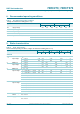
74HCT273
t
pd
propagation
delay
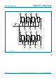
CP to Qn; see Figure 7
[1]
V
CC
= 4.5 V - 16 30 - 38 - 45 ns
V
CC
= 5.0 V; C
L
=15pF - 15 - - - - - ns
t
PHL
HIGH to LOW
propagation
delay
MR to Qn; see Figure 8
V
CC
= 4.5 V - 23 34 - 43 - 51 ns
V
CC
= 5.0 V; C
L
=15pF - 20 - - - - - ns
t
t
transition time Qn output; see Figure 7
[2]
V
CC
= 4.5 V - 7 15 - 19 - 22 ns
t
W
pulse width CP input; see Figure 7
V
CC
= 4.5 V 16 9 - 20 - 24 - ns
MR
input LOW;
see Figure 8
V
CC
= 4.5 V 16 8 - 20 - 24 - ns
t
rec
recovery time MR to CP; see Figure 8
V
CC
= 4.5 V 10 2 - 13 - 15 - ns
t
su
set-up time Dn to CP; see Figure 9
V
CC
= 4.5 V 12 5 - 15 - 18 - ns
t
h
hold time Dn to CP; see Figure 9
V
CC
= 4.5 V 3 4- 3 - 3 - ns
f
max
maximum
frequency
CP input; see Figure 7
V
CC
= 4.5 V 30 56 - 24 - 20 - MHz
V
CC
= 5.0 V; C
L
=15pF - 36 - - - - - MHz
C
PD
power
dissipation
capacitance
per package;
V
I
=GNDtoV
CC
1.5 V
[3]
-23- - - - - pF
Table 7. Dynamic characteristics
…continued
GND (ground = 0 V); C
L
= 50 pF unless otherwise specified; for test circuit, see Figure 10
Symbol Parameter Conditions 25 C 40 C to +85 C 40 C to +125 C Unit
Min Typ Max Min Max Min Max