
Datasheet


74HC_HCT27 All information provided in this document is subject to legal disclaimers. © NXP B.V. 2013. All rights reserved.
Product data sheet Rev. 4 — 5 June 2013 8 of 17
NXP Semiconductors
74HC27; 74HCT27
Triple 3-input NOR gate
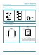
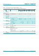
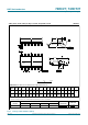
Test data is given in Table 9.
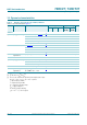
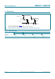
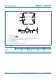
Definitions test circuit:
R
T
= Termination resistance should be equal to output impedance Z
o
of the pulse generator.
C
L
= Load capacitance including jig and probe capacitance.
R
L
= Load resistance.
S1 = Test selection switch
Fig 7. Test circuit for measuring switching times
V
M
V
M
t
W
t
W
10 %
90 %
0 V
V
I
V
I
negative
pulse
positive
pulse
0 V
V
M
V
M
90 %
10 %
t
f
t
r
t
r
t
f
001aad983
DUT
V
CC
V
CC
V
I
V
O
R
T
R
L
S1
C
L
open
G
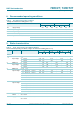
Table 9. Test data
Type Input Load S1 position
V
I
t
r
, t
f
C
L
R
L
t
PHL
, t
PLH
74HC27 V
CC
6ns 15pF, 50 pF 1k open
74HCT27 3V 6ns 15pF, 50 pF 1k open