
Datasheet


74HC_HCT30 All information provided in this document is subject to legal disclaimers. © NXP B.V. 2012. All rights reserved.
Product data sheet Rev. 6 — 27 December 2012 7 of 16
NXP Semiconductors
74HC30; 74HCT30
8-input NAND gate
[1] t
pd
is the same as t
PHL
and t
PLH
.
[2] t
t
is the same as t
THL
and t
TLH
.
[3] C
PD
is used to determine the dynamic power dissipation (P
D
in W):
P
D
=C
PD
V
CC
2
f
i
N+ (C
L
V
CC
2
f
o
) where:
f
i
= input frequency in MHz;
f
o
= output frequency in MHz;
C
L
= output load capacitance in pF;
V
CC
= supply voltage in V;
N = number of inputs switching;
(C
L
V
CC
2
f
o
) = sum of outputs.
11. Waveforms
C
PD
power dissipation
capacitance
per package; V
I
=GNDtoV
CC
[3]
-15- - -pF
74HCT30
t
pd
propagation delay A, B, C, D, E, F, G, H to Y;
see Figure 5
[1]
V
CC
= 4.5 V - 16 28 35 42 ns
V
CC
= 5.0 V; C
L
=15pF - 12 - - - ns
t
t
transition time V
CC
= 4.5 V; see Figure 5
[2]
- 7 15 19 22 ns
C
PD
power dissipation
capacitance
per package;
V
I
=GNDtoV
CC
1.5 V
[3]
-15- - -pF
Table 7. Dynamic characteristics
…continued
GND = 0 V; C
L
= 50 pF; for load circuit see Figure 6.
Symbol Parameter Conditions 25 C 40 C to +125 C Unit
Min Typ Max Max
(85 C)
Max
(125 C)
Measurement points are given in Table 8.
V
OL
and V
OH
are typical voltage output levels that occur with the output load.
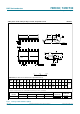
Fig 5. Input to output propagation delays
001aal792
V
OL
V
OH
GND
V
M
t
PHL
t
PLH
t
THL
t
TLH
V
M
V
X
V
Y
nY output
A, B, C, D,
E, F, G, H
input
V
I
Table 8. Measurement points
Type Input Output
V
M
V
M
V
X
V
Y
74HC30 0.5V
CC
0.5V
CC
0.1V
CC
0.9V
CC
74HCT30 1.3 V 1.3 V 0.1V
CC
0.9V
CC