
Datasheet


74HC_HCT3G06 All information provided in this document is subject to legal disclaimers. © NXP B.V. 2013. All rights reserved.
Product data sheet Rev. 4 — 19 December 2013 5 of 14
NXP Semiconductors 74HC3G06; 74HCT3G06
Triple inverter with open-drain outputs
[1] Typical values are measured at T
amb
=25C.
11. Dynamic characteristics
74HCT3G06
V
IH
HIGH-level input
voltage
V
CC
= 4.5 V to 5.5 V 2.0 1.6 - 2.0 - V
V
IL
LOW-level input
voltage
V
CC
= 4.5 V to 5.5 V - 1.2 0.8 - 0.8 V
V
OL
LOW-level output
voltage
V
I
= V
IH
or V
IL
I
O
= 20 A; V
CC
= 4.5 V - 0 0.1 - 0.1 V
I
O
= 4.0 mA; V
CC
= 4.5 V - 0.15 0.33 - 0.4 V
I
I
input leakage
current
V
I
=V
CC
or GND; V
CC
=5.5V - - 1.0 - 1.0 A
I
LO
output leakage
current
V
I
=V
IL
; V
O
=V
CC
or GND - - 5.0 - 10 A
I
CC
supply current per input pin; V
CC
=5.5V;
V
I
=V
CC
or GND; I
O
=0A;
--10 - 20A
I
CC
additional supply
current
per input; V
CC
= 4.5 V to 5.5 V;
V
I
=V
CC
2.1 V; I
O
=0A
- - 375 - 410 A
C
I
input capacitance - 1.5 - - - pF
Table 7. Static characteristics
…continued
Voltages are referenced to GND (ground = 0 V). All typical values are measured at T
amb
=25
C.
Symbol Parameter Conditions 40 C to +85 C 40 C to +125 C Unit
Min Typ
[1]
Max Min Max
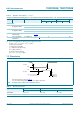
Table 8. Dynamic characteristics
Voltages are referenced to GND (ground = 0 V); all typical values are measured at T
amb
=25
C; for test circuit see Figure 7.
Symbol Parameter Conditions 40 C to +85 C 40 C to +125 C Unit
Min Typ Max Min Max
74HC3G06
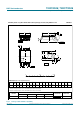
t
PZL
OFF-state to LOW
propagation delay
nA to nY; see Figure 6
V
CC
= 2.0 V - 22 95 - 125 ns
V
CC
= 4.5 V - 9 18 - 25 ns
V
CC
= 6.0 V - 8 16 - 20 ns
t
PLZ
LOW to OFF-state
propagation delay
nA to nY; see Figure 6
V
CC
= 2.0 V - 24 95 - 125 ns
V
CC
= 4.5 V - 11 20 - 27 ns
V
CC
= 6.0 V - 10 19 - 23 ns
t
THL
HIGH to LOW output
transition time
nY; see Figure 6
V
CC
= 2.0 V - 18 95 - 125 ns
V
CC
= 4.5 V - 6 19 - 25 ns
V
CC
= 6.0 V - 5 16 - 20 ns
C
PD
power dissipation
capacitance
V
I
=GNDtoV
CC
[1]
-4- - -pF