
Datasheet


74HC_HCT4017 All information provided in this document is subject to legal disclaimers. © NXP B.V. 2013. All rights reserved.
Product data sheet Rev. 4 — 10 December 2013 12 of 24
NXP Semiconductors 74HC4017; 74HCT4017
Johnson decade counter with 10 decoded outputs
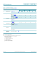
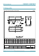
11. Waveforms
Measurement points are given in Table 8.
V
OL
and V
OH
are typical voltage output levels that occur with the output load.
Fig 8. Waveforms showing the set-up and hold times for CP0 to CP1 and CP1 to CP0
t
h
t
su
CP0 input
GND
GND
CP1 input
V
M
V
I
V
I
t
h
t
su
V
M
001aah245
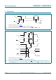
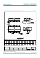
Measurement points are given in Table 8.
V
OL
and V
OH
are typical voltage output levels that occur with the output load.
Fig 9. Waveforms showing the minimum pulse width for CP0, CP1 and MR input; the maximum frequency for
CP0 and CP1 input; the recovery time for MR and the MR input to Qn and Q5-9 output propagation delays
CP0 input
V
I
GND
V
I
GND
V
I
GND
V
OH
V
OL
V
OH
V
OL
Q1 - Q9
output
MR input
CP1 input
V
M
V
M
1/f
max
t
W
t
W
t
rec
V
M
1/f
max
t
W
t
PLH
t
PHL
V
M
V
M
001aah246
Q0, Q5 - Q9
output