
Datasheet


74HC_HCT4094 All information provided in this document is subject to legal disclaimers. © NXP B.V. 2012. All rights reserved.
Product data sheet Rev. 6 — 31 December 2012 12 of 23
NXP Semiconductors
74HC4094; 74HCT4094
8-stage shift-and-store bus register
[2] t
en
is the same as t
PZH
and t
PZL
.
[3] t
dis
is the same as t
PLZ
and t
PHZ
.
[4] t
t
is the same as t
THL
and t
TLH
.
[5] C
PD
is used to determine the dynamic power dissipation (P
D
in W).
P
D
=C
PD
V
CC
2
f
i
N+(C
L
V
CC
2
f
o
) where:
f
i
= input frequency in MHz;
f
o
= output frequency in MHz;
C
L
= output load capacitance in pF;
V
CC
= supply voltage in V;
N = number of inputs switching;
(C
L
V
CC
2
f
o
) = sum of outputs.
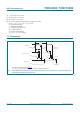
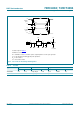
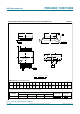
12. Waveforms
Measurement points are given in Table 8.
V
OL
and V
OH
are typical voltage output levels that occur with the output load.
Fig 8. Propagation delay input (CP) to output (QPn, QS1, QS2), output transition time, clock input (CP) pulse
width and the maximum frequency (CP)
1/f
max
t
W
t
PHL
t
PLH
V
I
GND
V
OH
V
OL
QPn, QS1 output
CP input
V
M
V
M
90 %
10 %
aaa-003132
t
PHL
t
PLH
t
TLH
t
THL
V
OH
V
OL
QS2 output
V
M