
Datasheet


74HC_HCT4094 All information provided in this document is subject to legal disclaimers. © NXP B.V. 2012. All rights reserved.
Product data sheet Rev. 6 — 31 December 2012 4 of 23
NXP Semiconductors
74HC4094; 74HCT4094
8-stage shift-and-store bus register
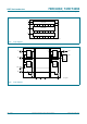
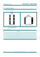
6. Pinning information
6.1 Pinning
6.2 Pin description
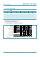
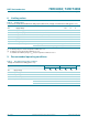
Fig 5. Pin configuration DIP16 and SO16 Fig 6. Pin configuration SSOP16 and TSSOP16
74HC4094
74HCT4094
STR V
CC
DOE
CP QP4
QP0 QP5
QP1 QP6
QP2 QP7
QP3 QS2
GND QS1
001aan577
1
2
3
4
5
6
7
8
10
9
12
11
14
13
16
15
74HC4094
74HCT4094
STR V
CC
DOE
CP QP4
QP0 QP5
QP1 QP6
QP2 QP7
QP3 QS2
GND QS1
001aan578
1
2
3
4
5
6
7
8
10
9
12
11
14
13
16
15
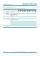
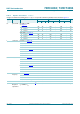
Table 2. Pin description
Symbol Pin Description
STR 1 strobe input
D 2 data input
CP 3 clock input
QP0 to QP7 4, 5, 6, 7, 14, 13, 12, 11 parallel output
V
SS
8 ground supply voltage
QS1, QS2 9, 10 serial output
OE 15 output enable input
V
DD
16 supply voltage