
Datasheet


74HC_HCT4094 All information provided in this document is subject to legal disclaimers. © NXP B.V. 2012. All rights reserved.
Product data sheet Rev. 6 — 31 December 2012 5 of 23
NXP Semiconductors
74HC4094; 74HCT4094
8-stage shift-and-store bus register
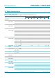
7. Functional description
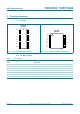
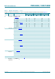
[1] At the positive clock edge, the information in the 7th register stage is transferred to the 8th register stage and the QSn outputs.
H = HIGH voltage level; L = LOW voltage level; X = don’t care;
= positive-going transition; = negative-going transition;
Z = HIGH-impedance OFF-state; NC = no change;
Q6S = the data in register stage 6 before the LOW to HIGH clock transition;
Q7S = the data in register stage 7 before the HIGH to LOW clock transition.
Table 3. Function table
[1]
Inputs Parallel outputs Serial outputs
CP OE STR D QP0 QPn QS1 QS2
LXXZZQ6SNC
LXXZZNCQ7S
HLXNCNCQ6SNC
HHLL QPn 1Q6S NC
HHHHQPn 1Q6S NC
H H H NCNCNCQ7S
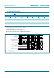
Fig 7. Timing diagram
001aaf117
CLOCK INPUT
DATA INPUT
STROBE INPUT
OUTPUT ENABLE INPUT
INTERNAL Q0S (FF 0)
OUTPUT QP0
INTERNAL Q6S (FF 6)
OUTPUT QP6
SERIAL OUTPUT QS1
SERIAL OUTPUT QS2
Z-state
Z-state