
Datasheet


74HC_HCT4094 All information provided in this document is subject to legal disclaimers. © NXP B.V. 2012. All rights reserved.
Product data sheet Rev. 6 — 31 December 2012 8 of 23
NXP Semiconductors
74HC4094; 74HCT4094
8-stage shift-and-store bus register
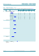
I
I
input leakage
current
V
I
=V
CC
or GND;
V
CC
=5.5V
--0.1 - 1.0 - 1.0 A
I
OZ
OFF-state
output current
V
I
=V
IH
or V
IL
; V
CC
=5.5V;
V
O
=V
CC
or GND per input
pin; other inputs at V
CC
or
GND; I
O
=0A
--0.5 - 5.0 - 10 A
I
CC
supply current V
I
=V
CC
or GND; I
O
=0A;
V
CC
=5.5V
- - 8.0 - 80 - 160 A
I
CC
additional
supply current
V
I
=V
CC
2.1 V;
other inputs at V
CC
or GND;
V
CC
= 4.5 V to 5.5 V;
I
O
=0A
per input pin; STR input - 100 360 - 450 - 490 A
per input pin; OE input - 150 540 - 675 - 735 A
per input pin; CP input - 150 540 - 675 - 735 A
per input pin; D input - 40 144 - 180 - 196 A
C
I
input
capacitance
-3.5- pF
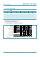
Table 6. Static characteristics
…continued
At recommended operating conditions; voltages are referenced to GND (ground = 0 V).
Symbol Parameter Conditions 25 C 40 C to +85 C 40 C to +125 C Unit
Min Typ Max Min Max Min Max