74HC594; 74HCT594 8-bit shift register with output register Rev. 03 — 20 December 2006 Product data sheet 1. General description The 74HC594; 74HCT594 is a high-speed Si-gate CMOS device and is pin compatible with Low-Power Schottky TTL (LSTTL). The 74HC594; 74HCT594 is an 8-bit, non-inverting, serial-in, parallel-out shift register that feeds an 8-bit D-type storage register. Separate clocks (SHCP and STCP) and direct overriding clears (SHR and STR) are provided on both the shift and storage registers.
74HC594; 74HCT594 NXP Semiconductors 8-bit shift register with output register 4. Ordering information Table 1. Ordering information Type number Package Temperature range Name Description Version 74HC594D −40 °C to +125 °C SO16 plastic small outline package; 16 leads; body width 3.9 mm SOT109-1 74HC594DB −40 °C to +125 °C SSOP16 plastic shrink small outline package; 16 leads; body width 5.
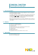
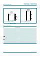
74HC594; 74HCT594 NXP Semiconductors 8-bit shift register with output register SHCP STCP STR 11 12 STCP Q7S 9 DS SHR R2 12 C2 10 R1 SRG8 11 15 Q0 1 Q1 2 Q2 3 Q3 2 4 Q4 3 5 Q5 4 6 Q6 7 Q7 14 10 13 SHR STR SHCP DS C1/ 14 1D 15 2D 1 5 6 7 9 mbc319 Q0 Q1 Q2 Q3 Q4 Q5 Q6 Q7 Q7S mbc322 Fig 2. Logic symbol Fig 3.
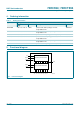
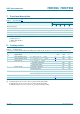
74HC594; 74HCT594 NXP Semiconductors 8-bit shift register with output register SHCP DS STCP SHR STR Q0 Q1 Q6 Q7 Q7S mbc323 Fig 5. Timing diagram 6. Pinning information 6.1 Pinning 74HC594 74HCT594 Q1 1 16 VCC Q2 2 15 Q0 Q3 3 14 DS Q4 4 13 STR Q5 5 12 STCP Q6 6 11 SHCP Q7 7 10 SHR GND 8 9 Q7S 001aaf611 Fig 6. Pin configuration SO16 74HC_HCT594_3 Product data sheet © NXP B.V. 2006. All rights reserved. Rev.
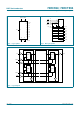
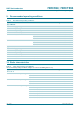
74HC594; 74HCT594 NXP Semiconductors 8-bit shift register with output register 74HC594 74HCT594 74HC594 74HCT594 Q1 1 16 VCC Q2 2 15 Q0 Q3 3 14 DS Q1 1 16 VCC Q2 2 15 Q0 Q4 4 13 STR Q3 3 14 DS Q5 5 12 STCP Q4 4 13 STR Q5 5 12 STCP Q6 6 11 SHCP Q6 6 11 SHCP Q7 7 10 SHR Q7 7 10 SHR GND 8 GND 8 9 Q7S 9 Q7S 001aaf614 001aaf613 Fig 7. Pin configuration SSOP16 Fig 8. Pin configuration DIP16 6.2 Pin description Table 2.
74HC594; 74HCT594 NXP Semiconductors 8-bit shift register with output register 7. Functional description Table 3.
4HC594; 74HCT594 NXP Semiconductors 8-bit shift register with output register 9. Recommended operating conditions Table 5. Recommended operating conditions Symbol Parameter Conditions Min Typ Max Unit Type 74HC594 VCC supply voltage 2.0 5.0 6.0 V VI input voltage 0 - VCC V VO output voltage 0 - VCC V Tamb ambient temperature −40 +25 +125 °C tr rise time VCC = 2.0 V - - 1000 ns VCC = 4.5 V - 6.0 500 ns VCC = 6.0 V - - 400 ns VCC = 2.
74HC594; 74HCT594 NXP Semiconductors 8-bit shift register with output register Table 6. Static characteristics type 74HC594 …continued At recommended operating conditions; voltages are referenced to GND (ground = 0 V). Symbol Parameter Conditions Min Typ Max Unit VOL LOW-level output voltage VI = VIH or VIL IO = 4.0 mA; VCC = 4.5 V - 0.15 0.26 V IO = 5.2 mA; VCC = 6.0 V - 0.16 0.26 V IO = 6.0 mA; VCC = 4.5 V - 0.15 0.26 V Serial data output Q7S Parallel data outputs IO = 7.
74HC594; 74HCT594 NXP Semiconductors 8-bit shift register with output register Table 6. Static characteristics type 74HC594 …continued At recommended operating conditions; voltages are referenced to GND (ground = 0 V). Symbol Parameter Conditions Min Typ Max Unit VIL LOW-level input voltage VCC = 2.0 V - - 0.5 V VCC = 4.5 V - - 1.35 V VCC = 6.0 V - - 1.8 V IO = −4.0 mA; VCC = 4.5 V 3.7 - - V IO = −5.2 mA; VCC = 6.0 V 5.2 - - V IO = −6.0 mA; VCC = 4.5 V 3.
74HC594; 74HCT594 NXP Semiconductors 8-bit shift register with output register Table 7. Static characteristics type 74HCT594 At recommended operating conditions; voltages are referenced to GND (ground = 0 V). Symbol Parameter Conditions Min Typ Max Unit Tamb = 25 °C VIH HIGH-level input voltage VCC = 4.5 V to 5.5 V 2.0 1.6 - V VIL LOW-level input voltage VCC = 4.5 V to 5.5 V - 1.2 0.8 V VOH HIGH-level output voltage VI = VIH or VIL 3.98 4.32 - V 3.98 4.32 - V - 0.15 0.
74HC594; 74HCT594 NXP Semiconductors 8-bit shift register with output register Table 7. Static characteristics type 74HCT594 …continued At recommended operating conditions; voltages are referenced to GND (ground = 0 V). Symbol Parameter Conditions Min Typ Max Unit ∆ICC additional supply current per input pin; VI = VCC − 2.1 V and other inputs at VCC or GND; IO = 0 A; VCC = 4.5 V to 5.5 V pins SHR, SHCP, STCP, STR - - 675 µA pin DS - - 112.
74HC594; 74HCT594 NXP Semiconductors 8-bit shift register with output register 11. Dynamic characteristics Table 8. Dynamic characteristics type 74HC594 GND = 0 V; tr = tf = 6 ns; CL = 50 pF; see Figure 15. Symbol tpd Parameter propagation delay 25 °C Conditions −40 °C to +85 °C −40 °C to +125 °C Unit Min Typ Max Min Max Min Max VCC = 2.0 V - 44 150 - 185 - 225 ns VCC = 4.5 V - 16 30 - 37 - 45 ns VCC = 5.0 V; CL = 15 pF - 13 - - - - - ns VCC = 6.
74HC594; 74HCT594 NXP Semiconductors 8-bit shift register with output register Table 8. Dynamic characteristics type 74HC594 …continued GND = 0 V; tr = tf = 6 ns; CL = 50 pF; see Figure 15. Symbol Parameter 25 °C Conditions Min tTLH −40 °C to +85 °C −40 °C to +125 °C Unit Typ Max Min Max Min Max 19 75 - 95 - 110 ns 7 15 - 19 - 22 ns - 6 13 - 16 - 19 ns VCC = 2.0 V - 14 60 - 75 - 90 ns VCC = 4.5 V - 5 12 - 15 - 18 ns VCC = 6.
74HC594; 74HCT594 NXP Semiconductors 8-bit shift register with output register Table 8. Dynamic characteristics type 74HC594 …continued GND = 0 V; tr = tf = 6 ns; CL = 50 pF; see Figure 15. Symbol tsu Parameter set-up time 25 °C Conditions −40 °C to +85 °C −40 °C to +125 °C Unit Min Typ Max Min Max Min Max VCC = 2.0 V 100 10 - 125 - 150 - ns VCC = 4.5 V 20 4 - 25 - 30 - ns VCC = 6.0 V 17 3 - 21 - 26 - ns VCC = 2.0 V 100 14 - 125 - 150 - ns VCC = 4.
74HC594; 74HCT594 NXP Semiconductors 8-bit shift register with output register Table 8. Dynamic characteristics type 74HC594 …continued GND = 0 V; tr = tf = 6 ns; CL = 50 pF; see Figure 15. Symbol CPD Parameter power dissipation capacitance 25 °C Conditions VI = GND to VCC; VCC = 5 V; fi = 1 MHz [2] −40 °C to +85 °C −40 °C to +125 °C Unit Min Typ Max Min Max Min Max - 84 - - - - - [1] tpd is the same as tPHL and tPLH.
74HC594; 74HCT594 NXP Semiconductors 8-bit shift register with output register Table 9. Dynamic characteristics type 74HCT594 …continued GND = 0 V; VCC = 4.5 V; tr = tf = 6 ns; CL = 50 pF; see Figure 15.
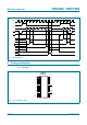
74HC594; 74HCT594 NXP Semiconductors 8-bit shift register with output register 12. Waveforms 1/fmax SHCP input VM tW tPLH Q7S output tPHL VM tTLH tTHL 001aae341 Measurement points are given in Table 10. tPLH and tPHL are the same as tpd. tTLH = LOW to HIGH output transition time; tTHL = HIGH to LOW output transition time. Fig 9.
74HC594; 74HCT594 NXP Semiconductors 8-bit shift register with output register VM SHCP input t su t su th th VM DS input VM Q7 output 001aae342 Measurement points are given in Table 10. The shaded areas indicate when the input is permitted to change for predictable output performance. Fig 11. The data set-up time and hold times for DS input to SHCP SHR input VM tsu STCP input VM Qn outputs VM mbc326 Measurement points are given in Table 10. Fig 12.
74HC594; 74HCT594 NXP Semiconductors 8-bit shift register with output register SHR input VM tW trec VM SHCP input tPHL VM Q7S output mbc324 Measurement points are given in Table 10. tPLH and tPHL are the same as tpd. Fig 13. The shift reset (SHR) pulse width, the shift reset to output (Q7S) propagation delay and the shift reset to shift clock (SHCP) recovery time STR input VM tW trec VM STCP input tPHL Qn outputs VM mbc325 Measurement points are given in Table 10.
74HC594; 74HCT594 NXP Semiconductors 8-bit shift register with output register VI tW 90 % negative pulse VM 0V tf tr tr tf VI 90 % positive pulse 0V VM 10 % VM VM 10 % tW VCC VCC PULSE GENERATOR VI VO RL S1 open DUT RT CL 001aad983 Test data is given in Table 11.
74HC594; 74HCT594 NXP Semiconductors 8-bit shift register with output register 13. Package outline SO16: plastic small outline package; 16 leads; body width 3.9 mm SOT109-1 D E A X c y HE v M A Z 16 9 Q A2 A (A 3) A1 pin 1 index θ Lp 1 L 8 e 0 detail X w M bp 2.5 5 mm scale DIMENSIONS (inch dimensions are derived from the original mm dimensions) UNIT A max. A1 A2 A3 bp c D (1) E (1) e HE L Lp Q v w y Z (1) mm 1.75 0.25 0.10 1.45 1.25 0.25 0.49 0.36 0.25 0.
74HC594; 74HCT594 NXP Semiconductors 8-bit shift register with output register SSOP16: plastic shrink small outline package; 16 leads; body width 5.3 mm D SOT338-1 E A X c y HE v M A Z 9 16 Q A2 A (A 3) A1 pin 1 index θ Lp L 8 1 detail X w M bp e 0 2.5 5 mm scale DIMENSIONS (mm are the original dimensions) UNIT A max. A1 A2 A3 bp c D (1) E (1) e HE L Lp Q v w y Z (1) θ mm 2 0.21 0.05 1.80 1.65 0.25 0.38 0.25 0.20 0.09 6.4 6.0 5.4 5.2 0.65 7.9 7.6 1.
74HC594; 74HCT594 NXP Semiconductors 8-bit shift register with output register DIP16: plastic dual in-line package; 16 leads (300 mil) SOT38-4 ME seating plane D A2 A A1 L c e Z w M b1 (e 1) b b2 MH 9 16 pin 1 index E 1 8 0 5 10 mm scale DIMENSIONS (inch dimensions are derived from the original mm dimensions) UNIT A max. A1 min. A2 max. b b1 b2 c D (1) E (1) e e1 L ME MH w Z (1) max. mm 4.2 0.51 3.2 1.73 1.30 0.53 0.38 1.25 0.85 0.36 0.23 19.50 18.55 6.
74HC594; 74HCT594 NXP Semiconductors 8-bit shift register with output register 14. Abbreviations Table 12. Abbreviations Acronym Description CMOS Complementary Metal Oxide Semiconductor DUT Device Under Test ESD ElectroStatic Discharge HBM Human Body Model LSTTL Low-Power Schottky Transistor-Transistor Logic MM Machine Model TTL Transistor-Transistor Logic 15. Revision history Table 13.
74HC594; 74HCT594 NXP Semiconductors 8-bit shift register with output register 16. Legal information 16.1 Data sheet status Document status[1][2] Product status[3] Definition Objective [short] data sheet Development This document contains data from the objective specification for product development. Preliminary [short] data sheet Qualification This document contains data from the preliminary specification. Product [short] data sheet Production This document contains the product specification.
NXP Semiconductors 74HC594; 74HCT594 8-bit shift register with output register 18. Contents 1 2 3 4 5 6 6.1 6.2 7 8 9 10 11 12 13 14 15 16 16.1 16.2 16.3 16.4 17 18 General description . . . . . . . . . . . . . . . . . . . . . . 1 Features . . . . . . . . . . . . . . . . . . . . . . . . . . . . . . . 1 Applications . . . . . . . . . . . . . . . . . . . . . . . . . . . . 1 Ordering information . . . . . . . . . . . . . . . . . . . . . 2 Functional diagram . . . . . . . . . . . . . . . . . . . . . .