
Datasheet


74HC_HCT594_3 © NXP B.V. 2006. All rights reserved.
Product data sheet Rev. 03 — 20 December 2006 15 of 26
NXP Semiconductors
74HC594; 74HCT594
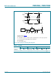
8-bit shift register with output register
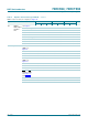
[1] t
pd
is the same as t
PHL
and t
PLH
.
[2] C
PD
is used to determine the dynamic power dissipation (P
D
in µW):
P
D
=C
PD
× V
CC
2
× f
i
× N+∑(C
L
× V
CC
2
× f
o
) where:
f
i
= input frequency in MHz;
f
o
= output frequency in MHz;
C
L
= output load capacitance in pF;
V
CC
= supply voltage in V;
N = number of inputs switching;
∑(C
L
× V
CC
2
× f
o
) = sum of outputs.
C
PD
power
dissipation
capacitance
V
I
= GND to V
CC
;
V
CC
=5V;
f
i
= 1 MHz
[2]
-84- - - - -pF
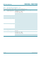
Table 8. Dynamic characteristics type 74HC594
…continued
GND = 0 V; t
r
= t
f
= 6 ns; C
L
= 50 pF; see Figure 15.
Symbol Parameter Conditions 25 °C −40 °C to +85 °C −40 °C to +125 °C Unit
Min Typ Max Min Max Min Max
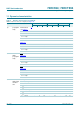
Table 9. Dynamic characteristics type 74HCT594
GND = 0 V;
V
CC
= 4.5 V;
t
r
= t
f
= 6 ns; C
L
= 50 pF; see Figure 15.
Symbol Parameter Conditions 25 °C −40 °C to +85 °C −40 °C to +125 °C Unit
Min Typ Max Min Max Min Max
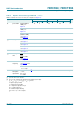
t
pd
propagation
delay
SHCP to Q7S;
see
Figure 9
[1]
- 18 32 - 40 - 48 ns
V
CC
= 5.0 V;
C
L
= 15 pF
-15- - - - -ns
STCP to Qn; see
Figure 10
- 18 32 - 40 - 48 ns
V
CC
= 5.0 V;
C
L
= 15 pF
-15- - - - -ns
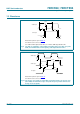
t
PHL
HIGH to
LOW
propagation
delay
SHR to Q7S; see
Figure 13
- 17 30 - 38 - 45 ns
V
CC
= 5.0 V;
C
L
= 15 pF
-14- - - - -ns
STR to Qn; see
Figure 14
- 17 30 - 38 - 45 ns
V
CC
= 5.0 V;
C
L
= 15 pF
-14- - - - -ns
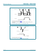
t
THL
HIGH to
LOW output
transition
time
see
Figure 9
Serial data output Q7S
V
CC
= 4.5 V - 7 15 - 19 - 22 ns
Parallel data outputs
V
CC
= 4.5 V - 5 12 - 15 - 18 ns
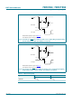
t
TLH
LOW to
HIGH output
transition
time
see
Figure 9
Serial data output Q7S
V
CC
= 4.5 V - 7 15 - 19 - 22 ns
Parallel data outputs
V
CC
= 4.5 V - 5 12 - 15 - 18 ns