
Datasheet

74HC_HCT594_3 © NXP B.V. 2006. All rights reserved.
Product data sheet Rev. 03 — 20 December 2006 6 of 26
NXP Semiconductors
74HC594; 74HCT594
8-bit shift register with output register
7. Functional description
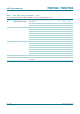
[1] H = HIGH voltage level;
L = LOW voltage level;
↑ = LOW-to-HIGH transition;
X = don’t care.
8. Limiting values
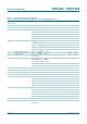
[1] The input and output voltage ratings may be exceeded if the input and output current ratings are observed.
[2] For DIP16 packages: above 70 °C the value of P
tot
derates linearly with 12 mW/K.
For SO16 packages: above 70 °C the value of P
tot
derates linearly with 8 mW/K.
For SSOP16 packages: above 60 °C the value of P
tot
derates linearly with 5.5 mW/K.
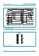
Table 3. Function table
[1]
Function Input
SHR STR SHCP STCP DS
Clear shift register L X X X X
Clear storage register X L X X X
Load DS into shift register stage 0, advance previous stage data to the next stage H X ↑ X H or L
Transfer shift register data to storage register and outputs Qn X H X ↑ X
Shift register one count pulse ahead of storage register H H ↑↑X
Table 4. Limiting values
In accordance with the Absolute Maximum Rating System (IEC 60134). Voltages are referenced to GND (ground = 0 V).
Symbol Parameter Conditions Min Max Unit
V
CC
supply voltage −0.5 +7.0 V
I
IK
input clamping current V
I
< −0.5 V or V
I
>V
CC
+ 0.5 V
[1]
- ±20 mA
I
OK
output clamping current V
O
< −0.5 V or V
O
> V
CC
+ 0.5 V
[1]
- ±20 mA
I
O
output current V
O
= −0.5 V to V
CC
+ 0.5 V
Serial data output Q7S - ±25 mA
Parallel data output - ±35 mA
I
CC
supply current Serial data output Q7S - 50 mA
Parallel data output - 70 mA
I
GND
ground current Serial data output Q7S - −50 mA
Parallel data output - −70 mA
T
stg
storage temperature −65 +150 °C
P
tot
total power dissipation T
amb
= −40 °C to +125 °C
[2]
- 500 mW