
Datasheet
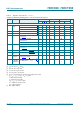

74HC_HCT595 All information provided in this document is subject to legal disclaimers. © NXP Semiconductors N.V. 2015. All rights reserved.
Product data sheet Rev. 7 — 26 January 2015 12 of 24
NXP Semiconductors
74HC595; 74HCT595
8-bit serial-in, serial or parallel-out shift register with output latches; 3-state
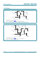
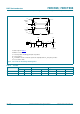
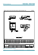
12. Waveforms
Measurement points are given in Table 8.
V
OL
and V
OH
are typical output voltage levels that occur with the output load.
Fig 9. Shift clock pulse, maximum frequency and input to output propagation delays
PQD
6+&3
LQSXW
46RXWSXW
W
3/+
W
3+/
W
:
I
PD[
9
0
9
2+
9
,
*1'
9
2/
9
0
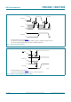
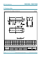
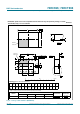
Measurement points are given in Table 8.
V
OL
and V
OH
are typical output voltage levels that occur with the output load.
Fig 10. Storage clock to output propagation delays
PQD
67&3
LQSXW
4QRXWSXW
W
3/+
W
3+/
W
:
W
VX
I
PD[
9
0
9
2+
9
,
*1'
9
2/
9
0
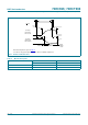
6+&3
LQSXW
9
,
*1'
9
0