
Datasheet


74HC_HCT595 All information provided in this document is subject to legal disclaimers. © NXP Semiconductors N.V. 2015. All rights reserved.
Product data sheet Rev. 7 — 26 January 2015 5 of 24
NXP Semiconductors
74HC595; 74HCT595
8-bit serial-in, serial or parallel-out shift register with output latches; 3-state
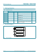
6.2 Pin description
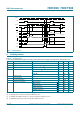
7. Functional description
[1] H = HIGH voltage state;
L = LOW voltage state;
= LOW-to-HIGH transition;
X = don’t care;
NC = no change;
Z = high-impedance OFF-state.
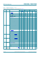
Table 2. Pin description
Symbol Pin Description
Q1 1 parallel data output 1
Q2 2 parallel data output 2
Q3 3 parallel data output 3
Q4 4 parallel data output 4
Q5 5 parallel data output 5
Q6 6 parallel data output 6
Q7 7 parallel data output 7
GND 8 ground (0 V)
Q7S 9 serial data output
MR
10 master reset (active LOW)
SHCP 11 shift register clock input
STCP 12 storage register clock input
OE
13 output enable input (active LOW)
DS 14 serial data input
Q0 15 parallel data output 0
V
CC
16 supply voltage
Table 3. Function table
[1]
Control Input Output Function
SHCP STCP OE MR DS Q7S Qn
X X L L X L NC a LOW-level on MR
only affects the shift registers
X L L X L L empty shift register loaded into storage register
X X H L X L Z shift register clear; parallel outputs in high-impedance OFF-state
X L H H Q6S NC logic HIGH-level shifted into shift register stage 0. Contents of all
shift register stages shifted through, e.g. previous state of stage 6
(internal Q6S) appears on the serial output (Q7S).
X L H X NC QnS contents of shift register stages (internal QnS) are transferred to
the storage register and parallel output stages
L H X Q6S QnS contents of shift register shifted through; previous contents of the
shift register is transferred to the storage register and the parallel
output stages