
Datasheet


74HC_HCT74 All information provided in this document is subject to legal disclaimers. © NXP B.V. 2012. All rights reserved.
Product data sheet Rev. 4 — 27 August 2012 10 of 21
NXP Semiconductors
74HC74; 74HCT74
Dual D-type flip-flop with set and reset; positive edge-trigger
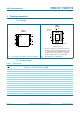
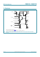
11. Waveforms
Measurement points are given in Table 9.
V
OL
and V
OH
are typical voltage output levels that occur with the output load.
Fig 7. Input to output propagation delay, output transition time, clock input pulse width and maximum
frequency
W
K
W
VX
W
VX
W
K
W
3+/
W
3+/
W
:
W
3/+
W
3/+
I
PD[
9
0
9
0
9
0
9
0
9
,
9
,
9
2+
9
2+
9
2/
9
2/
*1'
*1'
Q'LQSXW
Q&3
LQSXW
Q4RXWSXW
DDD
Q4RXWSXW
W
7+/
W
7/+