
Datasheet


74HC_HCT74 All information provided in this document is subject to legal disclaimers. © NXP B.V. 2012. All rights reserved.
Product data sheet Rev. 4 — 27 August 2012 4 of 21
NXP Semiconductors
74HC74; 74HCT74
Dual D-type flip-flop with set and reset; positive edge-trigger
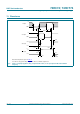
6. Functional description
[1] H = HIGH voltage level; L = LOW voltage level; X = don’t care.
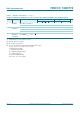
[1] H = HIGH voltage level; L = LOW voltage level; = LOW-to-HIGH transition; Q
n+1
= state after the next LOW-to-HIGH CP transition;
X = don’t care.
7. Limiting values
[1] For DIP14 package: P
tot
derates linearly with 12 mW/K above 70 C.
For SO14 package: P
tot
derates linearly with 8 mW/K above 70 C.
For (T)SSOP14 packages: P
tot
derates linearly with 5.5 mW/K above 60 C.
For DHVQFN14 packages: P
tot
derates linearly with 4.5 mW/K above 60 C.
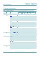
Table 3. Function table
[1]
Input Output
nSD nRD nCP nD nQ nQ
LHXXHL
HLXXLH
LLXXHH
Table 4. Function table
[1]
Input Output
nSD nRD nCP nD nQ
n+1
nQ
n+1
HH LLH
HH HHL
Table 5. Limiting values
In accordance with the Absolute Maximum Rating System (IEC 60134). Voltages are referenced to GND (ground = 0 V).
Symbol Parameter Conditions Min Max Unit
V
CC
supply voltage 0.5 +7 V
I
IK
input clamping current V
I
< 0.5 V or V
I
>V
CC
+0.5 V - 20 mA
I
OK
output clamping current V
O
< 0.5 V or V
O
>V
CC
+0.5V - 20 mA
I
O
output current V
O
= 0.5 V to (V
CC
+0.5V) - 25 mA
I
CC
supply current - +100 mA
I
GND
ground current 100 - mA
T
stg
storage temperature 65 +150 C
P
tot
total power dissipation DIP14 package
[1]
- 750 mW
SO14, (T)SSOP14 and DHVQFN14
packages
[1]
- 500 mW