
Datasheet

74HCT9046A_6 © NXP B.V. 2009. All rights reserved.
Product data sheet Rev. 06 — 15 September 2009 19 of 43
NXP Semiconductors
74HCT9046A
PLL with band gap controlled VCO
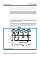
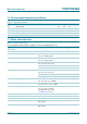
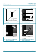
Fig 14. Typical input resistance curve at SIG_IN and
COMP_IN
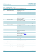
Fig 15. Input resistance at SIG_IN; COMP_IN with
∆V
I
= 0.5 V at self-bias point
___ R
s
= 50 kΩ
- - - R
s
= 300 kΩ
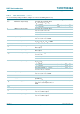
Fig 16. Input current at SIG_IN; COMP_IN with
∆V
I
= 0.5 V at self-bias point
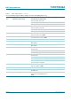
Fig 17. Offset voltage at demodulator output as a
function of VCO_IN and R
s
mbd108
self-bias operating point
V
I
∆V
I
I
I
800
600
200
0
400
mga956 - 1
V
I
(V)
(0.5 V
CC
) − 0.25 0.5 V
CC
(0.5 V
CC
) + 0.25
R
I
(kΩ)
5.5 V
V
CC
=
4.5 V
5
−5
0
mga957
V
I
(V)
(0.5 V
CC
) − 0.25 0.5 V
CC
(0.5 V
CC
) + 0.25
I
I
(µA)
4.5 V
V
CC
= 5.5V
5.5 V
4.5 V
40
−40
0
mga958
(0.5 V
CC
)
− 2 (0.5 V
CC
) + 20.5 V
CC
−20
20
60
V
offset
(mV)
V
VCO_IN
(V)
5.5 V
4.5 VV
CC
=