
Datasheet

74HCT9046A_6 © NXP B.V. 2009. All rights reserved.
Product data sheet Rev. 06 — 15 September 2009 34 of 43
NXP Semiconductors
74HCT9046A
PLL with band gap controlled VCO
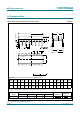
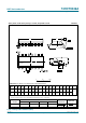
Using PC2 with the passive filter as shown in Figure 34 results in a high gain loop with the
same performance as a loop with an active filter. Hence loop filter equations as for a high
gain loop should be used. The current source output of PC2 can be simulated then with a
fictive filter resistance:
The transfer functions of the filter is given by:
Where:
The characteristic equation is:
This results in:
or:
This can be written as:
with the natural frequency ω
n
defined as:
and the damping value given as:
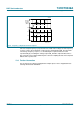
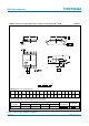
In Figure 35 the output frequency response to a step of input frequency is shown.
The overshoot and settling time percentages are now used to determine ω
n
.
From Figure 35 it can be seen that the damping ratio ζ = 0.707 will produce an overshoot
of less than 20 % and settle to within 5 % at ω
n
t = 5. The required settling time is 1 ms.
This results in:
K
p
5
4 π×
------------
0.4 V r⁄==
R3‘
R
bias
17
------------
=
K
f
1sτ
2
+
sτ
2
-----------------
=
τ
1
R3‘ C2×=
τ
2
R4 C2×=
1K
p
K
f
K
o
K
n
×××+
1K
p
1sτ
2
+
sτ
1
-----------------
+
K
v
s
------
K
n
0=
s
2
sK
p
K
v
K
n
τ
2
τ
1
-----
K
p
K
v
K
n
τ⁄
1
0=++
s
2
2ξω
n
s ω
n
()
2
0=++
ω
n
K
p
K
v
K
n
××
τ
1
---------------------------------=
ζ 0.5 τ
2
ω
n
××=