
Datasheet


74LV04_3 © NXP B.V. 2007. All rights reserved.
Product data sheet Rev. 03 — 4 December 2007 2 of 15
NXP Semiconductors
74LV04
Hex inverter
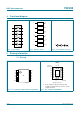
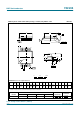
4. Functional diagram
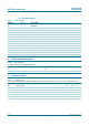
5. Pinning information
5.1 Pinning
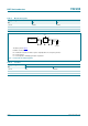
Fig 1. Logic symbol Fig 2. IEC logic symbol Fig 3. Logic diagram (one gate)
mna342
1A
1Y
1
2
2A
2Y
3
4
3A
3Y
5
6
4A
4Y
9
8
5A
5Y
11
10
6A
6Y
13
12
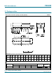
1
1
2
mna343
3
1
4
5
1
6
9
1
8
11
1
10
13
1
12
mna341
A
Y
(1) The die substrate is attached to this pad using
conductive die attach material. It can not be used as
a supply pin or input.
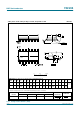
Fig 4. Pin configuration DIP14, SO14 and (T)SSOP14 Fig 5. Pin configuration DHVQFN14
04
1A V
CC
1Y 6A
2A 6Y
2Y 5A
3A 5Y
3Y 4A
GND 4Y
001aac441
1
2
3
4
5
6
7
8
10
9
12
11
14
13
001aah094
74LV04
Transparent top view
V
CC
(1)
3Y 4A
3A 5Y
2Y 5A
2A 6Y
1Y 6A
GND
4Y
1A
V
CC
6 9
5 10
4 11
3 12
2 13
7
8
1
14
terminal 1
index area