
Datasheet


74LV04_3 © NXP B.V. 2007. All rights reserved.
Product data sheet Rev. 03 — 4 December 2007 4 of 15
NXP Semiconductors
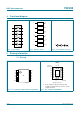
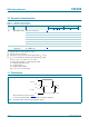
74LV04
Hex inverter
[1] The input and output voltage ratings may be exceeded if the input and output current ratings are observed.
[2] P
tot
derates linearly with 12 mW/K above 70 °C.
[3] P
tot
derates linearly with 8 mW/K above 70 °C.
[4] P
tot
derates linearly with 5.5 mW/K above 60 °C.
[5] P
tot
derates linearly with 4.5 mW/K above 60 °C.
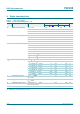
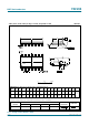
8. Recommended operating conditions
[1] The static characteristics are guaranteed from V
CC
= 1.2 V to V
CC
= 5.5 V, but LV devices are guaranteed to function down to
V
CC
= 1.0 V (with input levels GND or V
CC
).
P
tot
total power dissipation T
amb
= −40 °C to +125 °C
DIP14 package
[2]
- 750 mW
SO14 package
[3]
- 500 mW
(T)SSOP14 package
[4]
- 500 mW
DHVQFN14 package
[5]
- 500 mW
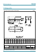
Table 4. Limiting values
…continued
In accordance with the Absolute Maximum Rating System (IEC 60134). Voltages are referenced to GND (ground = 0 V).
Symbol Parameter Conditions Min Max Unit
Table 5. Recommended operating conditions
Voltages are referenced to GND (ground = 0 V).
Symbol Parameter Conditions Min Typ Max Unit
V
CC
supply voltage
[1]
1.0 3.3 5.5 V
V
I
input voltage 0 - V
CC
V
V
O
output voltage 0 - V
CC
V
T
amb
ambient temperature −40 +25 +125 °C
∆t/∆V input transition rise and fall rate V
CC
= 1.0 V to 2.0 V - - 500 ns/V
V
CC
= 2.0 V to 2.7 V - - 200 ns/V
V
CC
= 2.7 V to 3.6 V - - 100 ns/V
V
CC
= 3.6 V to 5.5 V - - 50 ns/V