
Datasheet


9397 750 14501 © Koninklijke Philips Electronics N.V. 2005. All rights reserved.
Product data sheet Rev. 03 — 4 February 2005 4 of 21
Philips Semiconductors
74LV164
8-bit serial-in/parallel-out shift register
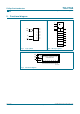
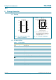
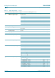
6. Pinning information
6.1 Pinning
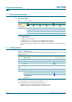
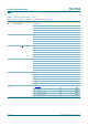
6.2 Pin description
(1) The die substrate is attached to the
exposed die pad using conductive die
attach material. It can not be used as
a supply pin or input.
Fig 4. Pin configuration DIP14, SO14,
SSOP14 and TSSOP14
Fig 5. Pin configuration DHVQFN14
74LV164
DSA V
CC
DSB Q7
Q0 Q6
Q1 Q5
Q2 Q4
Q3 MR
GND
CP
001aac422
1
2
3
4
5
6
7
8
10
9
12
11
14
13
001aac429
164
V
CC
(1)
Transparent top view
Q3 MR
Q2 Q4
Q1 Q5
Q0 Q6
DSB Q7
GND
CP
DSA
V
CC
6 9
5 10
4 11
3 12
2 13
7
8
1
14
terminal 1
index area
Table 3: Pin description
Symbol Pin Description
DSA 1 data input SA
DSB 2 data input SB
Q0 3 output 0
Q1 4 output 1
Q2 5 output 2
Q3 6 output 3
GND 7 ground (0 V)
CP 8 clock input (edge triggered LOW-to-HIGH)
MR 9 master reset input (active LOW)
Q4 10 output 4
Q5 11 output 5
Q6 12 output 6
Q7 13 output 7
V
CC
14 supply voltage