
Datasheet


74LV245_3 © NXP B.V. 2009. All rights reserved.
Product data sheet Rev. 03 — 15 April 2009 3 of 15
NXP Semiconductors
74LV245
Octal bus transceiver; 3-state
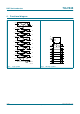
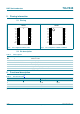
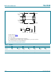
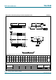
5. Pinning information
5.1 Pinning
5.2 Pin description
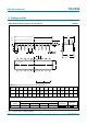
6. Functional description
[1] H = HIGH voltage level; L = LOW voltage level; X = don’t care; Z = high-impedance OFF-state.
Fig 3. Pin configuration DIP20, SO20 Fig 4. Pin configuration SSOP20, TSSOP20
74LV245
DIR V
CC
A0 OE
A1 B0
A2 B1
A3 B2
A4 B3
A5 B4
A6 B5
A7 B6
GND B7
001aaj962
1
2
3
4
5
6
7
8
9
10
12
11
14
13
16
15
18
17
20
19
74LV245
DIR V
CC
A0 OE
A1 B0
A2 B1
A3 B2
A4 B3
A5 B4
A6 B5
A7 B6
GND B7
001aaj963
1
2
3
4
5
6
7
8
9
10
12
11
14
13
16
15
18
17
20
19
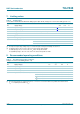
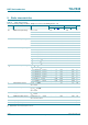
Table 2. Pin description
Symbol Pin Description
DIR 1 direction control
A0 to A7 2, 3, 4, 5, 6, 7, 8, 9 data input/output
GND 10 ground (0 V)
B0 to B7 18, 17, 16, 15, 14, 13, 12, 11 data input/output
OE 19 output enable input (active LOW)
V
CC
20 supply voltage
Table 3. Function selection
[1]
Input Output/input
OE DIR An Bn
L L A = B input
L H input B = A
HXZZ