
Datasheet


74LV245_3 © NXP B.V. 2009. All rights reserved.
Product data sheet Rev. 03 — 15 April 2009 6 of 15
NXP Semiconductors
74LV245
Octal bus transceiver; 3-state
10. Dynamic characteristics
[1] All typical values are measured at T
amb
=25°C.
[2] t
pd
is the same as t
PLH
and t
PHL
.
t
en
is the same as t
PZL
and t
PZH
.
t
dis
is the same as t
PLZ
and t
PHZ
.
[3] Typical values are measured at nominal supply voltage (V
CC
= 3.3 V and V
CC
= 5.0 V).
[4] C
PD
is used to determine the dynamic power dissipation (P
D
in µW).
P
D
=C
PD
× V
CC
2
× f
i
× N+Σ(C
L
× V
CC
2
× f
o
) where:
f
i
= input frequency in MHz, f
o
= output frequency in MHz
C
L
= output load capacitance in pF
V
CC
= supply voltage in Volts
N = number of inputs switching
Σ(C
L
× V
CC
2
× f
o
) = sum of the outputs.
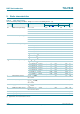
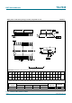
Table 7. Dynamic characteristics
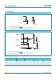
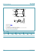
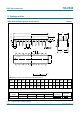
Voltages are referenced to GND (ground = 0 V). For test circuit see Figure 7.
Symbol Parameter Conditions −40 °C to +85 °C −40 °C to +125 °C Unit
Min Typ
[1]
Max Min Max
t
pd
propagation delay An, Bn to Bn, An; see Figure 5
[2]
V
CC
= 1.2 V - 45 28 - - ns
V
CC
= 2.0 V - 15 28 - 34 ns
V
CC
= 2.7 V - 11 19 - 24 ns
V
CC
= 3.0 V to 3.6 V; C
L
=15pF
[3]
-7- - -ns
V
CC
= 3.0 V to 3.6 V
[3]
- 9 16 - 20 ns
V
CC
= 4.5 V to 5.5 V
[3]
- 8 11 - 14 ns
t
en
enable time OE to An, Bn; see Figure 6
[2]
V
CC
= 1.2 V - 55 - - - ns
V
CC
= 2.0 V - 19 31 - 39 ns
V
CC
= 2.7 V - 14 23 - 29 ns
V
CC
= 3.0 V to 3.6 V
[3]
- 10 18 - 23 ns
V
CC
= 4.5 V to 5.5 V
[3]
- 8.5 14 - 18 ns
t
dis
disable time OE to An, Bn; see Figure 6
[2]
V
CC
= 1.2 V - 65 - - - ns
V
CC
= 2.0 V - 24 32 - 39 ns
V
CC
= 2.7 V - 18 24 - 29 ns
V
CC
= 3.0 V to 3.6 V
[3]
- 14 20 - 24 ns
V
CC
= 4.5 V to 5.5 V
[3]
- 11.5 16 - 19 ns
C
PD
power dissipation
capacitance
C
L
= 50 pF; f
i
= 1 MHz;
V
I
= GND to V
CC
; V
CC
= 3.3 V
[4]
-40- - -pF