
Datasheet

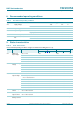
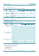


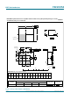
Table Of Contents
- 1. General description
- 2. Features and benefits
- 3. Ordering information
- 4. Functional diagram
- 5. Pinning information
- 6. Functional description
- 7. Limiting values
- 8. Recommended operating conditions
- 9. Static characteristics
- 10. Dynamic characteristics
- 11. Waveforms
- 12. Package outline
- 13. Abbreviations
- 14. Revision history
- 15. Legal information
- 16. Contact information
- 17. Contents

1. General description
The 74LVC07A provides six non-inverting buffers. The outputs are open-drain and can be
connected to other open-drain outputs to implement active-LOW wired-OR or active-HIGH
wired-AND functions.
Inputs can be driven from either 3.3 V or 5 V devices. This feature allows the use of these
devices as translators in mixed 3.3 V and 5 V applications.
2. Features and benefits
5 V tolerant inputs and outputs (open-drain) for interfacing with 5 V logic
Wide supply voltage range from 1.2 V to 5.5 V
CMOS low power consumption
Direct interface with TTL levels
Inputs accept voltages up to 5 V
Complies with JEDEC standard:
JESD8-7A (1.65 V to 1.95 V)
JESD8-5A (2.3 V to 2.7 V)
JESD8-C/JESD36 (2.7 V to 3.6 V)
ESD protection:
HBM JESD22-A114F exceeds 2000 V
MM JESD22-A115-B exceeds 200 V
CDM JESD22-C101E exceeds 1000 V
Specified from 40 C to +85 C and 40 C to +125 C
3. Ordering information
74LVC07A
Hex buffer with open-drain outputs
Rev. 5 — 27 October 2011 Product data sheet
Table 1. Ordering information
Type number Package
Temperature range Name Description Version
74LVC07AD 40 Cto+125C SO14 plastic small outline package; 14 leads;
body width 3.9 mm
SOT108-1
74LVC07APW 40 Cto+125C TSSOP14 plastic thin small outline package; 14 leads;
body width 4.4 mm
SOT402-1
74LVC07ABQ 40 Cto+125C DHVQFN14 plastic dual in-line compatible thermal enhanced very
thin quad flat package; no leads; 14 terminals;
body 2.5 3 0.85 mm
SOT762-1