
Datasheet

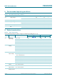
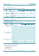


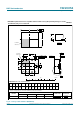
Table Of Contents
- 1. General description
- 2. Features and benefits
- 3. Ordering information
- 4. Functional diagram
- 5. Pinning information
- 6. Functional description
- 7. Limiting values
- 8. Recommended operating conditions
- 9. Static characteristics
- 10. Dynamic characteristics
- 11. Waveforms
- 12. Package outline
- 13. Abbreviations
- 14. Revision history
- 15. Legal information
- 16. Contact information
- 17. Contents

74LVC07A All information provided in this document is subject to legal disclaimers. © NXP B.V. 2011. All rights reserved.
Product data sheet Rev. 5 — 27 October 2011 5 of 14
NXP Semiconductors
74LVC07A
Hex buffer with open-drain outputs
[1] All typical values are measured at V
CC
= 3.3 V (unless stated otherwise) and T
amb
=25C.
10. Dynamic characteristics
[1] Typical values are measured at T
amb
=25C and V
CC
= 1.2 V, 1.8 V, 2.5 V, 2.7 V, 3.3 V and 5.0 V respectively.
[2] C
PD
is used to determine the dynamic power dissipation (P
D
in W).
P
D
=C
PD
V
CC
2
f
i
N+(C
L
V
CC
2
f
o
) where:
f
i
= input frequency in MHz; f
o
= output frequency in MHz
C
L
= output load capacitance in pF
V
CC
= supply voltage in Volts
N = number of inputs switching
(C
L
V
CC
2
f
o
) = sum of the outputs
I
CC
supply current V
I
=V
CC
or GND; I
O
=0A;
V
CC
= 5.5 V
-0.110-40A
I
CC
additional
supply current
per input pin;
V
I
=V
CC
0.6 V; I
O
=0A;
V
CC
= 2.7 V to 5.5 V
- 5 500 - 5000 A
C
I
input
capacitance
V
CC
= 0 V to 5.5 V;
V
I
=GNDtoV
CC
-5.0---pF
Table 6. Static characteristics
…continued
At recommended operating conditions. Voltages are referenced to GND (ground = 0 V).
Symbol Parameter Conditions 40 C to +85 C 40 C to +125 C Unit
Min Typ
[1]
Max Min Max
Table 7. Dynamic characteristics
Voltages are referenced to GND (ground = 0 V). For test circuit see Figure 7
.
Symbol Parameter Conditions 40 C to +85 C 40 C to +125 C Unit
Min Typ
[1]
Max Min Max
t
PZL
OFF-state to LOW
propagation delay
nA to nY; see Figure 6
V
CC
= 1.2 V - 8.0 - - - ns
V
CC
= 1.65 V to 1.95 V 0.5 1.7 5.5 0.5 6.5 ns
V
CC
= 2.3 V to 2.7 V 0.5 1.2 2.8 0.5 3.5 ns
V
CC
= 2.7 V 0.5 1.8 3.3 0.5 4.5 ns
V
CC
= 3.0 V to 3.6 V 0.5 1.2 3.6 0.5 4.5 ns
V
CC
= 4.5 V to 5.5 V 0.5 1.6 2.6 0.5 3.5 ns
t
PLZ
LOW to OFF-state
propagation delay
nA to nY; see Figure 6
V
CC
= 1.2 V - 10 - - - ns
V
CC
= 1.65 V to 1.95 V 0.5 3.0 5.5 0.5 6.5 ns
V
CC
= 2.3 V to 2.7 V 0.5 1.7 2.8 0.5 3.5 ns
V
CC
= 2.7 V 0.5 2.1 3.3 0.5 4.5 ns
V
CC
= 3.0 V to 3.6 V 0.5 2.5 3.6 0.5 4.5 ns
V
CC
= 4.5 V to 5.5 V 0.5 1.6 2.6 0.5 3.5 ns
C
PD
power dissipation
capacitance
per buffer; V
I
=GNDtoV
CC
[2]
V
CC
= 1.65 V to 1.95 V - 6.5 - - - pF
V
CC
= 2.3 V to 2.7 V - 6.9 - - - pF
V
CC
= 3.0 V to 3.6 V - 7.2 - - - pF