
Datasheet

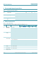
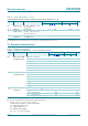


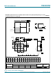
Table Of Contents
- 1. General description
- 2. Features and benefits
- 3. Ordering information
- 4. Functional diagram
- 5. Pinning information
- 6. Functional description
- 7. Limiting values
- 8. Recommended operating conditions
- 9. Static characteristics
- 10. Dynamic characteristics
- 11. Waveforms
- 12. Package outline
- 13. Abbreviations
- 14. Revision history
- 15. Legal information
- 16. Contact information
- 17. Contents

74LVC07A All information provided in this document is subject to legal disclaimers. © NXP B.V. 2011. All rights reserved.
Product data sheet Rev. 5 — 27 October 2011 6 of 14
NXP Semiconductors
74LVC07A
Hex buffer with open-drain outputs
11. Waveforms
Measurements points are given in Table 8.
Logic level: V
OL
is a typical output voltage level that occurs with the output load.
Fig 6. The input (nA) to output (nY) propagation delays
mna528
t
PLZ
V
X
nY output
nA input
V
I
V
CC
V
M
V
M
V
OL
GND
t
PZL
V
M
Table 8. Measurement points
Supply voltage Input Output
V
CC
V
M
V
X
< 2.7 V 0.5 V
CC
V
OL
+0.15V
2.7 V to 3.6 V 1.5 V V
OL
+0.3V
4.5 V to 5.5 V 0.5 V
CC
V
OL
+0.3V