
Datasheet


1. General description
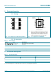
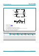
The 74LVC125A consists of four non-inverting buffers/line drivers with 3-state outputs
(nY) that are controlled by the output enable input (nOE
). A HIGH at nOE causes the
outputs to assume a high-impedance OFF-state.
Inputs can be driven from either 3.3 V or 5 V devices. When disabled, up to 5.5 V can be
applied to the outputs.
2. Features and benefits
5 V tolerant inputs/outputs for interfacing with 5 V logic
Wide supply voltage range from 1.2 V to 3.6 V
CMOS low power consumption
Direct interface with TTL levels
Complies with JEDEC standard:
JESD8-7A (1.65 V to 1.95 V)
JESD8-5A (2.3 V to 2.7 V)
JESD8-C/JESD36 (2.7 V to 3.6 V)
ESD protection:
HBM JESD22-A114F exceeds 2000 V
MM JESD22-A115-B exceeds 200 V
CDM JESD22-C101E exceeds 1000 V
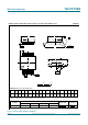
Multiple package options
Specified from 40 C to +85 C and 40 C to +125 C
74LVC125A
Quad buffer/line driver with 5 V tolerant input/outputs; 3-state
Rev. 7 — 11 April 2013 Product data sheet