
Datasheet


1. General description
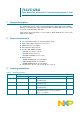
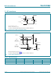
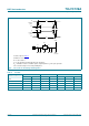
The 74LVC126A consists of four non-inverting buffers/line drivers with 3-state outputs,
which are controlled by the output enable input (nOE). A LOW at nOE causes the outputs
to assume a high-impedance OFF-state.
Inputs can be driven from either 3.3 V or 5 V devices. When disabled, up to 5.5 V can be
applied to the outputs.
2. Features and benefits
5 V tolerant inputs/outputs for interfacing with 5 V logic
Wide supply voltage range from 1.2 V to 3.6 V
CMOS low power consumption
Direct interface with TTL levels
Complies with JEDEC standard:
JESD8-7A (1.65 V to 1.95 V)
JESD8-5A (2.3 V to 2.7 V)
JESD8-C/JESD36 (2.7 V to 3.6 V)
ESD protection:
HBM JESD22-A114F exceeds 2000 V
MM JESD22-A115B exceeds 200 V
CDM JESD22-C101E exceeds 1000 V
Specified from 40 C to +85 C and 40 C to +125 C
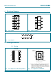
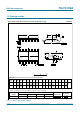
3. Ordering information
74LVC126A
Quad buffer/line driver with 5 V tolerant input/outputs; 3-state
Rev. 8 — 8 April 2014 Product data sheet
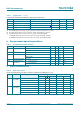
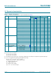
Table 1. Ordering information
Type number Package
Temperature range Name Description Version
74LVC126AD 40 Cto+125C SO14 plastic small outline package; 14 leads;
body width 3.9 mm
SOT108-1
74LVC126ADB 40 Cto+125C SSOP14 plastic shrink small outline package; 14 leads;
body width 5.3 mm
SOT337-1
74LVC126APW 40 Cto+125C TSSOP14 plastic thin small outline package; 14 leads;
body width 4.4 mm
SOT402-1
74LVC126ABQ 40 Cto+125C DHVQFN14 plastic dual in-line compatible thermal enhanced very
thin quad flat package; no leads; 14 terminals;
body 2.5 3 0.85 mm
SOT762-1