
Datasheet


74LVC126A All information provided in this document is subject to legal disclaimers. © NXP Semiconductors N.V. 2014. All rights reserved.
Product data sheet Rev. 8 — 8 April 2014 2 of 16
NXP Semiconductors
74LVC126A
Quad buffer/line driver with 5 V tolerant input/outputs; 3-state
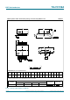
4. Functional diagram
5. Pinning information
5.1 Pinning
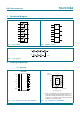
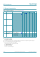
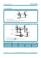
Fig 1. Logic symbol Fig 2. IEC logic symbol
mna235
1A 1Y
2
1
3
1OE
2A 2Y
5
4
6
2OE
3A 3Y
9
10
8
3OE
4A 4Y
12
13
11
4OE
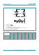
mna236
1
EN1
1
3
2
4
6
5
10
8
9
13
11
12
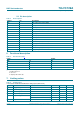
Fig 3. Logic diagram
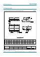
mna234
nOE
nA
nY
(1) This is not a supply pin. The substrate is attached to this
pad using conductive die attach material. There is no
electrical or mechanical requirement to solder this pad.
However, if it is soldered, the solder land should remain
floating or be connected to GND.
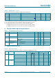
Fig 4. Pin configuration for SO14 and (T)SSOP14 Fig 5. Pin configuration for DHVQFN14
/9&$
2( 9
&&
$
2(
<
$
2( <
$
2(
<
$
*1' <
DDD
001aac983
126
Transparent top view
2Y 3A
2A 3OE
2OE 4Y
1Y 4A
1A 4OE
GND
3Y
1OE
V
CC
6 9
5 10
4 11
3 12
2 13
7
8
1
14
terminal 1
index area
GND
(1)