
Datasheet


74LVC126A All information provided in this document is subject to legal disclaimers. © NXP Semiconductors N.V. 2014. All rights reserved.
Product data sheet Rev. 8 — 8 April 2014 7 of 16
NXP Semiconductors
74LVC126A
Quad buffer/line driver with 5 V tolerant input/outputs; 3-state
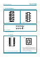
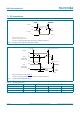
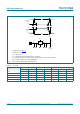
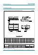
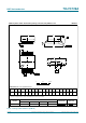
11. AC waveforms
V
M
=1.5VatV
CC
2.7 V;
V
M
=0.5 V
CC
at V
CC
<2.7V;
V
OL
and V
OH
are typical output voltage levels that occur with the output load.
Fig 6. The input nA to output nY propagation delays
mna237
t
PHL
t
PLH
V
M
V
M
nA input
nY output
GND
V
I
V
OH
V
OL
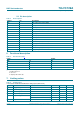
Measurement points are given in Table 8.
V
OL
and V
OH
are typical output voltage levels that occur with the output load.
Fig 7. 3-state enable and disable times
mna684
t
PLZ
t
PHZ
outputs
disabled
outputs
enabled
V
Y
V
X
outputs
enabled
output
LOW-to-OFF
OFF-to-LOW
output
HIGH-to-OFF
OFF-to-HIGH
nOE input
V
I
V
CC
V
M
V
OL
V
OH
GND
GND
t
PZL
t
PZH
V
M
V
M
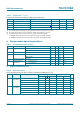
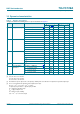
Table 8. Measurement points
Supply voltage Input Output
V
CC
V
M
V
M
V
X
V
Y
V
CC
<2.7V 0.5 V
CC
0.5 V
CC
V
OL
+0.15V V
OH
0.15 V
V
CC
2.7 V 1.5 V 1.5 V V
OL
+0.3V V
OH
0.3 V