
Datasheet

74LVC132A All information provided in this document is subject to legal disclaimers. © NXP B.V. 2011. All rights reserved.
Product data sheet Rev. 3 — 7 December 2011 4 of 16
NXP Semiconductors
74LVC132A
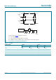
Quad 2-input NAND Schmitt trigger
7. Functional description
[1] H = HIGH voltage level;
L = LOW voltage level.
8. Limiting values
[1] The minimum input voltage ratings may be exceeded if the input current ratings are observed.
[2] The output voltage ratings may be exceeded if the output current ratings are observed.
[3] When V
CC
= 0 V (Power-down mode), the output voltage can be 3.6 V in normal operation.
[4] For SO14 packages: P
tot
derates linearly with 8 mW/K above 70 C.
For TSSOP14 packages: P
tot
derates linearly with 5.5 mW/K above 60 C.
For DHVQFN14 packages: P
tot
derates linearly with 4.5 mW/K above 60 C.
9. Recommended operating conditions
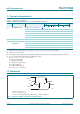
Table 3. Function table
[1]
Input Output
nA nB nY
LLH
LHH
HL H
HHL
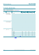
Table 4. Limiting values
In accordance with the Absolute Maximum Rating System (IEC 60134). Voltages are referenced to GND (ground = 0 V).
Symbol Parameter Conditions Min Max Unit
V
CC
supply voltage 0.5 +6.5 V
V
I
input voltage
[1]
0.5 +6.5 V
V
O
output voltage
[2][3]
0.5 V
CC
+ 0.5 V
I
IK
input clamping current V
I
< 0 V 50 - mA
I
OK
output clamping current V
O
> V
CC
or V
O
< 0 V - 50 mA
I
O
output current V
O
= 0 V to V
CC
- 50 mA
I
CC
supply current - 100 mA
I
GND
ground current 100 - mA
T
stg
storage temperature 65 +150 C
P
tot
total power dissipation T
amb
= 40 C to +125 C
[4]
-500 mW
Table 5. Recommended operating conditions
Symbol Parameter Conditions Min Typ Max Unit
V
CC
supply voltage 1.65 - 3.6 V
functional 1.2 - - V
V
I
input voltage 0 - 5.5 V
V
O
output voltage 0 - V
CC
V
T
amb
ambient temperature 40 - +125 C