
Datasheet

74LVC132A All information provided in this document is subject to legal disclaimers. © NXP B.V. 2011. All rights reserved.
Product data sheet Rev. 3 — 7 December 2011 7 of 16
NXP Semiconductors
74LVC132A
Quad 2-input NAND Schmitt trigger
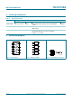
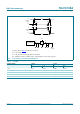
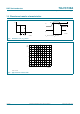
Test data is given in Table 8. Definitions for test circuit:
R
L
= Load resistance
C
L
= Load capacitance including jig and probe capacitance
R
T
= Termination resistance should be equal to output impedance Z
o
of the pulse generator.
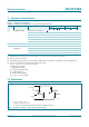
Fig 7. Load circuitry for measuring switching times
V
M
V
M
t
W
t
W
10 %
90 %
0 V
V
I
V
I
negative
pulse
positive
pulse
0 V
V
M
V
M
90 %
10 %
t
f
t
r
t
r
t
f
001aaf615
V
CC
V
I
V
O
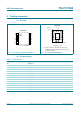
DUT
C
L
R
T
R
L
PULSE
GENERATOR
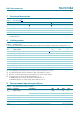
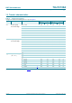
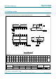
Table 8. Test data
Supply voltage Input Load
V
I
t
r
, t
f
C
L
R
L
1.2 V V
CC
2 ns 30 pF 1 k
1.65 V to 1.95 V V
CC
2 ns 30 pF 1 k
2.3 V to 2.7 V V
CC
2 ns 30 pF 500
2.7 V 2.7 V 2.5ns 50pF 500
3.0Vto3.6V 2.7V 2.5ns 50pF 500