
Datasheet


74LVC138A All information provided in this document is subject to legal disclaimers. © NXP B.V. 2011. All rights reserved.
Product data sheet Rev. 5 — 19 October 2011 7 of 16
NXP Semiconductors
74LVC138A
3-to-8 line decoder/demultiplexer; inverting
[1] Typical values are measured at T
amb
=25C and V
CC
= 1.2 V, 1.8 V, 2.5 V, 2.7 V, and 3.3 V respectively.
[2] t
pd
is the same as t
PLH
and t
PHL
.
[3] Skew between any two outputs of the same package switching in the same direction. This parameter is guaranteed by design.
[4] C
PD
is used to determine the dynamic power dissipation (P
D
in W).
P
D
=C
PD
V
CC
2
f
i
N+(C
L
V
CC
2
f
o
) where:
f
i
= input frequency in MHz; f
o
= output frequency in MHz
C
L
= output load capacitance in pF
V
CC
= supply voltage in V
N = number of inputs switching
(C
L
V
CC
2
f
o
) = sum of outputs
11. Waveforms
C
PD
power dissipation
capacitance
V
I
= GND to V
CC
[4]
V
CC
= 1.65 V to 1.95 V - 9.9 - pF
V
CC
= 2.3 V to 2.7 V - 15.8 - pF
V
CC
= 3.0 V to 3.6 V - 21.1 - pF
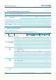
Table 7. Dynamic characteristics
…continued
Voltages are referenced to GND (ground = 0 V). For test circuit see Figure 8.
Symbol Parameter Conditions 40 C to +85 C 40 C to +125 C Unit
Min Typ
[1]
Max Min Max
V
M
=1.5VatV
CC
2.7 V;
V
M
=0.5 V
CC
at V
CC
<2.7V;
V
OL
and V
OH
are typical output voltage levels that occur
with the output load.
V
M
=1.5VatV
CC
2.7 V;
V
M
=0.5 V
CC
at V
CC
<2.7V;
V
OL
and V
OH
are typical output voltage levels that occur
with the output load.
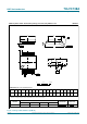
Fig 6. The inputs An, E3 to outputs Yn propagation
delays
Fig 7. The inputs En to outputs Yn propagation
delays
mna373
An, E3
input
Yn
output
t
PHL
t
THL
t
PLH
GND
V
CC
V
M
V
M
V
OH
V
OL
t
TLH
mna374
E1, E2
input
Yn
output
t
PHL
t
PLH
GND
V
CC
V
M
V
M
V
OH
V
OL
t
THL
t
TLH