
Datasheet


74LVC_LVCH16244A All information provided in this document is subject to legal disclaimers. © NXP B.V. 2014. All rights reserved.
Product data sheet Rev. 13 — 7 February 2014 6 of 19
NXP Semiconductors
74LVC16244A; 74LVCH16244A
16-bit buffer/line driver; 5 V input/output tolerant; 3-state
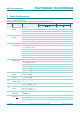
7. Limiting values
[1] The minimum input voltage ratings may be exceeded if the input current ratings are observed.
[2] The output voltage ratings may be exceeded if the output current ratings are observed.
[3] Above 60 C the value of P
tot
derates linearly with 5.5 mW/K.
[4] Above 70 C the value of P
tot
derates linearly with 1.8 mW/K.
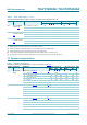
8. Recommended operating conditions
Table 4. Limiting values
In accordance with the Absolute Maximum Rating System (IEC 60134). Voltages are referenced to GND (ground = 0 V).
Symbol Parameter Conditions Min Max Unit
V
CC
supply voltage 0.5 +6.5 V
I
IK
input clamping current V
I
<0V 50 - mA
V
I
input voltage
[1]
0.5 +6.5 V
I
OK
output clamping current V
O
>V
CC
or V
O
<0V - 50 mA
V
O
output voltage output HIGH or LOW
[2]
0.5 V
CC
+0.5 V
output 3-state
[2]
0.5 +6.5 V
I
O
output current V
O
=0V toV
CC
- 50 mA
I
CC
supply current - 100 mA
I
GND
ground current 100 - mA
T
stg
storage temperature 65 +150 C
P
tot
total power dissipation T
amb
= 40 C to +125 C;
(T)SSOP48 package
[3]
-500mW
VFBGA56 package
[4]
-1000mW
HXQFN60 package
[4]
-1000mW
Table 5. Recommended operating conditions
Symbol Parameter Conditions Min Typ Max Unit
V
CC
supply voltage 1.65 - 3.6 V
functional 1.2 - 3.6 V
V
I
input voltage 0 - 5.5 V
V
O
output voltage output HIGH or LOW 0 - V
CC
V
output 3-state 0 - 5.5 V
T
amb
ambient temperature in free air 40 - +125 C
t/V input transition rise and fall rate V
CC
= 1.2 V to 2.7 V 0 - 20 ns/V
V
CC
= 2.7 V to 3.6 V 0 - 10 ns/V