
Datasheet

74LVC_LVCH16245A All information provided in this document is subject to legal disclaimers. © NXP B.V. 2012. All rights reserved.
Product data sheet Rev. 12 — 13 February 2012 10 of 20
NXP Semiconductors
74LVC16245A; 74LVCH16245A
16-bit bus transceiver with direction pin; 5 V tolerant; 3-state
[1] t
pd
is the same as t
PLH
and t
PHL
.
t
en
is the same as t
PZL
and t
PZH
.
t
dis
is the same as t
PLZ
and t
PHZ
.
[2] Typical values are measured at T
amb
=25C and V
CC
= 1.2 V, 1.8 V, 2.5 V, 2.7 V and 3.3 V respectively.
[3] C
PD
is used to determine the dynamic power dissipation (P
D
in W).
P
D
=C
PD
V
CC
2
f
i
N+(C
L
V
CC
2
f
o
) where:
f
i
= input frequency in MHz; f
o
= output frequency in MHz
C
L
= output load capacitance in pF
V
CC
= supply voltage in Volts
N = number of inputs switching
(C
L
V
CC
2
f
o
) = sum of the outputs.
11. Waveforms
t
dis
disable time nOE to nAn, nBn; see Figure 8
[1]
V
CC
= 1.2 V - 11.0 - - - ns
V
CC
= 1.65 V to 1.95 V 1.0 4.9 13.1 1.0 14.7 ns
V
CC
= 2.3 V to 2.7 V 0.5 2.7 7.1 0.5 7.9 ns
V
CC
= 2.7 V 1.5 3.4 6.6 1.5 8.5 ns
V
CC
= 3.0 V to 3.6 V 1.5 3.3 5.6 1.5 7.0 ns
C
PD
power
dissipation
capacitance
per input; V
I
=GNDtoV
CC
[3]
V
CC
= 1.65 V to 1.95 V - 11.5 - - - pF
V
CC
= 2.3 V to 2.7 V - 15.2 - - - pF
V
CC
= 3.0 V to 3.6 V - 18.5 - - - pF
Table 7. Dynamic characteristics
…continued
Voltages are referenced to GND (ground = 0 V). For test circuit see Figure 9.
Symbol Parameter Conditions 40 C to +85 C 40 C to +125 C Unit
Min Typ
[2]
Max Min Max
Measurement points are given in Table 8.
Logic levels: V
OL
and V
OH
are typical output voltage levels that occur with the output load.
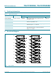
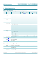
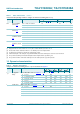
Fig 7. The input (nAn, nBn) to output (nBn, nAn) propagation delays
mna477
nAn, nBn
input
nBn, nAn
output
t
PHL
t
PLH
GND
V
I
V
M
V
M
V
OH
V
OL