
Datasheet

74LVC_LVCH16245A All information provided in this document is subject to legal disclaimers. © NXP B.V. 2012. All rights reserved.
Product data sheet Rev. 12 — 13 February 2012 6 of 20
NXP Semiconductors
74LVC16245A; 74LVCH16245A
16-bit bus transceiver with direction pin; 5 V tolerant; 3-state
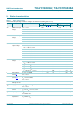
5.2 Pin description
6. Functional description
[1] H = HIGH voltage level; L = LOW voltage level; X = don’t care; Z = high-impedance OFF-state.
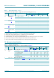
Table 2. Pin description
Symbol Pin Description
SOT370-1 and
SOT362-1
SOT702-1 SOT1134-2
1DIR, 2DIR 1, 24 A1, K1 A30, A13 direction control input
1B0 to 1B7 2, 3, 5, 6, 8, 9, 11,
12
B2, B1, C2, C1, D2, D1,
E2, E1
B20, A31, D5, D1, A2,
B2, B3, A5
data input/output
2B0 to 2B7 13, 14, 16, 17, 19,
20, 22, 23
F1, F2, G1, G2, H1, H2,
J1, J2
A6, B5, B6, A9, D2, D6,
A12, B8
data input/output
GND 4, 10, 15, 21, 28,
34, 39, 45
B3, B4, D3, D4, G3, G4,
J3, J4
A32, A3, A8, A11, A16,
A19, A24, A27
ground (0 V)
V
CC
7, 18, 31, 42 C3, C4, H3, H4 A1, A10, A17, A26 supply voltage
1OE
, 2OE 48, 25 A6, K6 A29, A14 output enable input (active LOW)
1A0 to 1A7 47, 46, 44, 43, 41,
40, 38, 37
B5, B6, C5, C6, D5, D6,
E5, E6
B18, A28, D8, D4, A25,
B16, B15, A22
data input/output
2A0 to 2A7 36, 35, 33, 32, 30,
29, 27, 26
F6, F5, G6, G5, H6, H5,
J6, J5
A21, B13, B12, A18, D3,
D7, A15, B10
data input/output
n.c. - A2, A3, A4, A5, K2, K3,
K4, K5
A4, A7, A20, A23, B1,
B4, B7, B9, B11, B14,
B17, B19
not connected
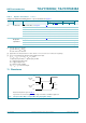
Table 3. Function table
[1]
Inputs Outputs
nOE nDIR nAn nBn
L L nAn = nBn inputs
L H inputs nBn = nAn
HXZZ