
Datasheet


74LVC1G10 All information provided in this document is subject to legal disclaimers. © NXP Semiconductors N.V. 2014. All rights reserved.
Product data sheet Rev. 4 — 10 September 2014 7 of 17
NXP Semiconductors
74LVC1G10
Single 3-input NAND gate
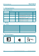
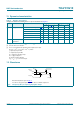
Table 9. Measurement points
Supply voltage Input Output
V
CC
V
M
V
M
1.65 V to 1.95 V 0.5V
CC
0.5V
CC
2.3 V to 2.7 V 0.5V
CC
0.5V
CC
2.7V 1.5V 1.5V
3.0V to 3.6V 1.5V 1.5V
4.5 V to 5.5 V 0.5V
CC
0.5V
CC
Test data is given in Table 10.
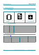
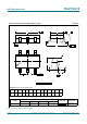
Definitions for test circuit:
R
L
= Load resistance.
C
L
= Load capacitance including jig and probe capacitance.
R
T
= Termination resistance should be equal to the output impedance Z
o
of the pulse generator.
V
EXT
= External voltage for measuring switching times.
Fig 8. Test circuit for measuring switching times
9
(;7
9
&&
9
,
9
2
PQD
'87
&
/
5
7
5
/
5
/
*
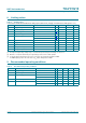
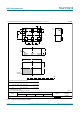
Table 10. Test data
Supply voltage Input Load V
EXT
V
CC
V
I
t
r
=t
f
C
L
R
L
t
PLH
, t
PHL
1.65 V to 1.95 V V
CC
2.0ns 30pF 1k open
2.3 V to 2.7 V V
CC
2.0ns 30pF 500 open
2.7V 2.7V 2.5ns 50pF 500 open
3.0V to 3.6V 2.7V 2.5ns 50pF 500 open
4.5 V to 5.5 V V
CC
2.5ns 50pF 500 open