
Datasheet


74LVC1G17 All information provided in this document is subject to legal disclaimers. © NXP B.V. 2012. All rights reserved.
Product data sheet Rev. 10 — 29 June 2012 3 of 21
NXP Semiconductors
74LVC1G17
Single Schmitt trigger buffer
6. Pinning information
6.1 Pinning
6.2 Pin description
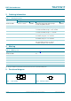
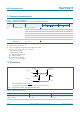
Fig 3. Logic diagram
mnb152
A
Y
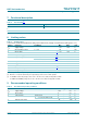
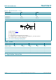
Fig 4. Pin configuration SOT353-1 and SOT753 Fig 5. Pin configuration SOT886
74LVC1G17
n.c. V
CC
A
GND Y
001aaf190
1
2
3
5
4
74LVC1G17
A
001aaf191
n.c.
GND
n.c.
V
CC
Y
Transparent top view
2
3
1
5
4
6
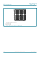
Fig 6. Pin configuration SOT891, SOT1115 and
SOT1202
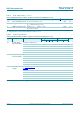
Fig 7. Pin configuration SOT1226 (X2SON5)
74LVC1G17
A
001aaf402
n.c.
GND
n.c.
V
CC
Y
Transparent top view
2
3
1
5
4
6
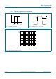
n.c.
V
CC
GND
1
3
2
5
4
A
Y
aaa-003025
Transparent top view
74LVC1G17
Table 3. Pin description
Symbol Pin Description
TSSOP5 and X2SON5 XSON6
n.c. 1 1, 5 not connected
A 2 2 data input
GND 3 3 ground (0 V)
Y 4 4 data output
V
CC
5 6 supply voltage