
Datasheet


1. General description
The 74LVC1G18 is a 1-of-2 non-inverting demultiplexer with a 3-state output. The device
buffers the data on input pin A and passes it either to output 1Y or 2Y, depending on
whether the state of the select input (pin S) is LOW or HIGH. Input can be driven from
either 3.3 or 5 V devices. These features allow the use of these devices in a mixed
3.3 and 5 V environment.
This device is fully specified for partial power-down applications using I
OFF
. The I
OFF
circuitry disables the output, preventing the damaging backflow current through the device
when it is powered down.
2. Features
n Wide supply voltage range from 1.65 to 5.5 V
n 5 V tolerant input/output for interfacing with 5 V logic
n High noise immunity
n Complies with JEDEC standard:
u JESD8-7 (1.65 V to 1.95 V)
u JESD8-5 (2.3 V to 2.7 V)
u JESD8B/JESD36 (2.7 V to 3.6 V)
n ESD protection:
u HBM EIA/JESD22-A114E exceeds 2000 V
u MM EIA/JESD22-A115-A exceeds 200 V.
n ±24 mA output drive (V
CC
= 3.0 V)
n CMOS low power consumption
n Latch-up performance exceeds 250 mA
n Direct interface with TTL levels
n SOT363 and SOT457 package
n Specified from −40 to +85 °C and −40 to +125 °C.
3. Ordering information
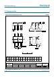
74LVC1G18
1-of-2 non-inverting demultiplexer with 3-state deselected
output
Rev. 02 — 30 August 2007 Product data sheet
Table 1. Ordering information
Type number Package
Temperature range Name Description Version
74LVC1G18GW −40 °C to +125 °C SC-88 plastic surface-mounted package; 6 leads SOT363
74LVC1G18GV −40 °C to +125 °C SC-74 plastic surface-mounted package (TSOP6); 5 leads SOT457