
Datasheet


74LVC1G332 All information provided in this document is subject to legal disclaimers. © NXP Semiconductors N.V. 2014. All rights reserved.
Product data sheet Rev. 5 — 10 September 2014 3 of 17
NXP Semiconductors
74LVC1G332
Single 3-input OR gate
6. Pinning information
6.1 Pinning
6.2 Pin description
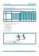
7. Functional description
[1] H = HIGH voltage level;
L = LOW voltage level;
X = don’t care.
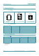
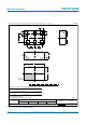
Fig 4. Pin configuration SOT363
and SOT457
Fig 5. Pin configuration SOT886 Fig 6. Pin configuration SOT891,
SOT1115 and SOT1202
74LVC1G332
AC
GND
BY
001aaf473
1
2
3
6
V
CC
5
4
74LVC1G332
GND
001aaf474
A
B
V
CC
C
Y
Transparent top view
2
3
1
5
4
6
74LVC1G332
GND
001aaf475
A
B
V
CC
C
Y
Transparent top view
2
3
1
5
4
6
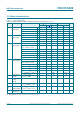
Table 3. Pin description
Symbol Pin Description
A 1 data input
GND 2 ground (0 V)
B 3 data input
Y 4 data output
V
CC
5 supply voltage
C 6 data input
Table 4. Function table
[1]
Input Output
A B C Y
HXXH
XHXH
XXHH
LLLL