
Datasheet


74LVC1G79 All information provided in this document is subject to legal disclaimers. © NXP B.V. 2012. All rights reserved.
Product data sheet Rev. 11 — 2 July 2012 4 of 21
NXP Semiconductors
74LVC1G79
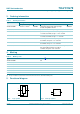
Single D-type flip-flop; positive-edge trigger
6.2 Pin description
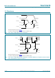
7. Functional description
[1] H = HIGH voltage level;
L = LOW voltage level;
= LOW-to-HIGH CP transition;
X = don’t care;
q = lower case letter indicates the state of referenced input, one set-up time prior to the LOW-to-HIGH CP transition.
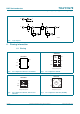
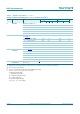
Table 3. Pin description
Symbol Pin Description
TSSOP5 and X2SON5 XSON6
D 1 1 data input
CP 2 2 clock pulse input
GND 3 3 ground (0 V)
Q 4 4 data output
n.c. - 5 not connected
V
CC
5 6 supply voltage
Table 4. Function table
[1]
Input Output
CP D Q
LL
HH
LXq