
Datasheet


74LVC1G79 All information provided in this document is subject to legal disclaimers. © NXP B.V. 2012. All rights reserved.
Product data sheet Rev. 11 — 2 July 2012 9 of 21
NXP Semiconductors
74LVC1G79
Single D-type flip-flop; positive-edge trigger
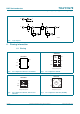
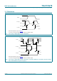
12. Waveforms
Measurement points are given in Table 9.
V
OL
and V
OH
are typical output voltage levels that occur with the output.
Fig 8. Clock (CP) to output (Q) propagation delay times
mna443
CP input
Q output
t
PHL
t
PLH
V
M
V
M
V
OH
V
I
GND
D input
V
I
GND
V
OL
V
M
V
M
Measurement points are given in Table 9.
V
OL
and V
OH
are typical output voltage levels that occur with the output.
Fig 9. Clock (CP) to output (Q) propagation delay times, clock pulse width, D to set-up times, the CP to D hold
times and maximum clock pulse frequency
mna647
t
h
t
su
t
h
t
PHL
t
W
t
PLH
t
su
1/f
max
V
M
V
M
V
M
V
I
GND
V
I
GND
CP input
D input
V
OH
V
OL
Q output