
Datasheet


74LVC1G80 All information provided in this document is subject to legal disclaimers. © NXP B.V. 2012. All rights reserved.
Product data sheet Rev. 12 — 2 July 2012 3 of 21
NXP Semiconductors
74LVC1G80
Single D-type flip-flop; positive-edge trigger
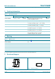
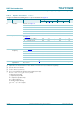
6. Pinning information
6.1 Pinning
Fig 3. Logic diagram
mna651
CP
D
C
C
C
C
C
C
C
C
C
TG
TG
TG
TG
C
Q
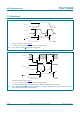
Fig 4. Pin configuration SOT353-1 and SOT753 Fig 5. Pin configuration SOT886
74LVC1G80
DV
CC
CP
GND Q
001aab662
1
2
3
5
4
74LVC1G80
CP
001aab663
D
GND
n.c.
V
CC
Q
Transparent top view
2
3
1
5
4
6
Fig 6. Pin configuration SOT891, SOT1115 and
SOT1202
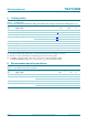
Fig 7. Pin configuration SOT1226 (X2SON5)
74LVC1G80
CP
001aaf535
D
GND
n.c.
V
CC
Q
Transparent top view
2
3
1
5
4
6
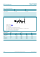
D
V
CC
GND
1
3
2
5
4
CP
Q
aaa-003030
Transparent top view
74LVC1G80