
Datasheet


74LVC1G86 All information provided in this document is subject to legal disclaimers. © NXP B.V. 2012. All rights reserved.
Product data sheet Rev. 10 — 2 July 2012 7 of 19
NXP Semiconductors
74LVC1G86
2-input EXCLUSIVE-OR gate
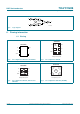
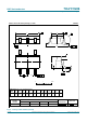
12. Waveforms
Measurement points are given in Table 9.
V
OL
and V
OH
are typical output voltage levels that occur with the output.
Fig 8. The input A and B to output Y propagation delay times
mna041
t
PHL
t
PLH
V
M
V
M
A, B
input
Y
output
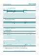
Table 9. Measurement points
Supply voltage Input Output
V
CC
V
M
V
M
1.65 V to 1.95 V 0.5V
CC
0.5V
CC
2.3 V to 2.7 V 0.5V
CC
0.5V
CC
2.7V 1.5V 1.5V
3.0V to 3.6V 1.5V 1.5V
4.5 V to 5.5 V 0.5V
CC
0.5V
CC