
Datasheet


74LVC1GX04 All information provided in this document is subject to legal disclaimers. © NXP B.V. 2013. All rights reserved.
Product data sheet Rev. 3 — 21 August 2013 11 of 18
NXP Semiconductors
74LVC1GX04
X-tal driver
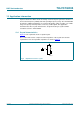
13.1.1 Design
Figure 10 shows the recommended way to connect a crystal to the 74LVC1GX04. This
circuit is basically a Pierce oscillator circuit in which the crystal is operating at its
fundamental frequency. The parallel load capacitance of C
1
and C
2
tune the circuit. C
1
and C
2
are in series with the crystal and they should be equal (approximately). R
1
is the
drive-limiting resistor. It is set to approximately the same value as the reactance of C
1
at
the crystal frequency (R
1
=X
C1
). This setting results in an input to the crystal of 50 % of
the rail-to-rail output of X2. It keeps the drive level into the crystal within drive
specifications and the designer should verify it. Overdriving the crystal can cause
damage.
The feedback resistor (R
f
= 1 M) provides negative feedback. It sets a bias point of the
inverter near mid-supply, operating the 74LVC1GU04 portion in the high gain linear
region.
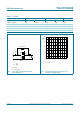
(1) resonance
(2) anti-resonance
(3) load resonance
Fig 9. Reactance and resistance characteristics of a crystal
mnb104
C
0
C
1
R
1
L
1
C
0
C
1
R
1
L
1
C
0
C
1
R
1
L
1
C
L
R
1
f
r
f
r
f
resistance
reactance
f
a
R
L
f
L
f
resistance
reactance
f
a
R
p
f
L
f
resistance
reactance
f
a
0
+
−
0
+
−
0
+
−
∞
∞
∞
(1)
(2)
(3)
C
L