
Datasheet


74LVC1GX04 All information provided in this document is subject to legal disclaimers. © NXP B.V. 2013. All rights reserved.
Product data sheet Rev. 3 — 21 August 2013 12 of 18
NXP Semiconductors
74LVC1GX04
X-tal driver
To calculate the values of C
1
and C
2
, the designer can use the formula:
C
L
is the load capacitance as specified by the crystal manufacturer. C
s
is the stray
capacitance of the circuit (for the 74LVC1GX04 it is equal to an input capacitance of 5 pF).
13.1.2 Testing
After the calculations are performed for a particular crystal, the oscillator circuit should be
tested. The following simple checks verify the prototype design of a crystal controlled
oscillator circuit. Perform the checks after laying out the board:
• Test the oscillator over worst-case conditions (lowest supply voltage, worst-case
crystal and highest operating temperature). Adding series and parallel resistors can
simulate a worst-case crystal.
• Insure that the circuit does not oscillate without the crystal.
• Check the frequency stability over a supply range greater than that which is likely to
occur during normal operation.
• Check that the start-up time is within system requirements.
As the 74LVC1GX04 isolates the system loading, once the design is optimized, the single
layout may work in multiple applications for any given crystal.
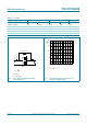
Fig 10. Crystal oscillator configuration for the 74LVC1GX04
C
L
C
1
C
2
C
1
C
2
+
-------------------
C
s
+=
mnb103
R
f
74LVC1GU04
portion
74LVC1G04
portion
system load
Xtal C
1
R
sys
C
sys
C
2
X2
Y
X1