
Datasheet

74LVC1GX04 All information provided in this document is subject to legal disclaimers. © NXP B.V. 2013. All rights reserved.
Product data sheet Rev. 3 — 21 August 2013 3 of 18
NXP Semiconductors
74LVC1GX04
X-tal driver
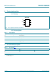
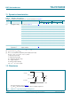
6. Pinning information
6.1 Pinning
6.2 Pin description
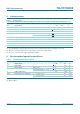
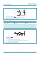
7. Functional description
[1] H = HIGH voltage level;
L = LOW voltage level.
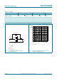
Fig 2. Pin configuration SOT363 and SOT457
74LVC1GX04
n.c. Y
GND
X1 X2
001aag401
1
2
3
6
V
CC
5
4
Table 3. Pin description
Symbol Pin Description
n.c. 1 not connected
GND 2 ground (0 V)
X1 3 data input
X2 4 data output
V
CC
5 supply voltage
Y 6 data output
Table 4. Function table
[1]
Input Output
X1 X2 Y
HL H
LHL