
Datasheet

74LVC1GX04 All information provided in this document is subject to legal disclaimers. © NXP B.V. 2013. All rights reserved.
Product data sheet Rev. 3 — 21 August 2013 4 of 18
NXP Semiconductors
74LVC1GX04
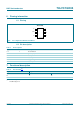
X-tal driver
8. Limiting values
[1] The minimum input and output voltage ratings may be exceeded if the input and output current ratings are observed.
[2] When V
CC
= 0 V (Power-down mode), the output voltage can be 5.5 V in normal operation.
[3] Above 87.5 C the value of P
tot
derates linearly with 4.0 mW/K.
9. Recommended operating conditions
[1] For use of a regular crystal oscillator, the recommended minimum V
CC
should be 2.0 V.
[2] Only for output Y.
Table 5. Limiting values
In accordance with the Absolute Maximum Rating System (IEC 60134). Voltages are referenced to GND (ground = 0 V).
Symbol Parameter Conditions Min Max Unit
V
CC
supply voltage 0.5 +6.5 V
I
IK
input clamping current V
I
<0V 50 - mA
V
I
input voltage
[1]
0.5 +6.5 V
I
OK
output clamping current V
O
>V
CC
or V
O
<0V - 50 mA
V
O
output voltage Active mode
[1][2]
0.5 V
CC
+ 0.5 V
Power-down mode
[1][2]
0.5 +6.5 V
I
O
output current V
O
=0VtoV
CC
- 50 mA
I
CC
supply current - 100 mA
I
GND
ground current 100 - mA
T
stg
storage temperature 65 +150 C
P
tot
total power dissipation T
amb
= 40 Cto+125C
[3]
-250 mW
Table 6. Recommended operating conditions
Symbol Parameter Conditions Min Typ Max Unit
V
CC
supply voltage
[1]
1.65 - 5.5 V
V
I
input voltage 0 - 5.5 V
V
O
output voltage Active mode
[2]
0-V
CC
V
Power-down mode; V
CC
=0V 0 - 5.5 V
T
amb
ambient temperature 40 - +125 C
t/V input transition rise and fall rate V
CC
= 1.65 V to 2.7 V - - 20 ns/V
V
CC
= 2.7 V to 5.5 V - - 10 ns/V