
Datasheet

74LVC1GX04 All information provided in this document is subject to legal disclaimers. © NXP B.V. 2013. All rights reserved.
Product data sheet Rev. 3 — 21 August 2013 8 of 18
NXP Semiconductors
74LVC1GX04
X-tal driver
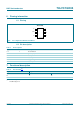
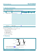
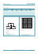
Measurement points are given in Table 9.
V
OL
and V
OH
are typical output voltage levels that occur with the output load.
Fig 4. Input X1 to output Y propagation delay times
mnb100
X1 input
Y output
t
PHL
t
PLH
GND
V
I
V
M
V
M
V
OH
V
OL
Table 9. Measurement points
Supply voltage Input Output
V
CC
V
M
V
M
1.65 V to 1.95 V 0.5 V
CC
0.5 V
CC
2.3 V to 2.7 V 0.5 V
CC
0.5 V
CC
2.7V 1.5V 1.5V
3.0V to3.6V 1.5V 1.5V
4.5 V to 5.5 V 0.5 V
CC
0.5 V
CC
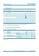
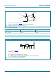
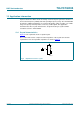
Test data is given in Table 10.
Definitions test circuit:
R
L
= Load resistance.
C
L
= Load capacitance including jig and probe capacitance.
R
T
= Termination resistance should be equal to output impedance Z
o
of the pulse generator.
V
EXT
= External voltage for measuring switching times.
Fig 5. Test circuit for measuring switching times
V
EXT
V
CC
V
I
V
O
mna616
DUT
C
L
R
T
R
L
R
L
G