
Datasheet


74LVC_LVCH244A All information provided in this document is subject to legal disclaimers. © NXP B.V. 2013. All rights reserved.
Product data sheet Rev. 8 — 26 June 2013 5 of 19
NXP Semiconductors
74LVC244A; 74LVCH244A
Octal buffer/line driver; 3-state
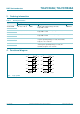
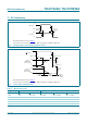
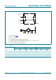
6. Functional description
[1] H = HIGH voltage level; L = LOW voltage level; X = don’t care; Z = high-impedance OFF-state.
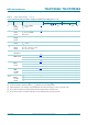
7. Limiting values
[1] The minimum input voltage ratings may be exceeded if the input current ratings are observed.
[2] The output voltage ratings may be exceeded if the output current ratings are observed.
[3] For SO20 packages: above 70 C derate linearly with 8 mW/K.
For (T)SSOP20 packages: above 60 C derate linearly with 5.5 mW/K.
For DHVQFN20 and DHXQFN20 packages: above 60 C derate linearly with 4.5 mW/K.
Table 3. Function table
[1]
Control Input Output
nOE nAn nYn
LLL
LHH
HXZ
Table 4. Limiting values
In accordance with the Absolute Maximum Rating System (IEC 60134). Voltages are referenced to GND (ground = 0 V).
Symbol Parameter Conditions Min Max Unit
V
CC
supply voltage 0.5 +6.5 V
I
IK
input clamping current V
I
<0V 50 - mA
V
I
input voltage
[1]
0.5 +6.5 V
I
OK
output clamping current V
O
>V
CC
or V
O
<0V - 50 mA
V
O
output voltage output HIGH or LOW
[2]
0.5 V
CC
+0.5 V
output 3-state
[2]
0.5 +6.5 V
I
O
output current V
O
=0V toV
CC
- 50 mA
I
CC
supply current - 100 mA
I
GND
ground current 100 - mA
T
stg
storage temperature 65 +150 C
P
tot
total power dissipation T
amb
= 40 C to +125 C
[3]
-500mW